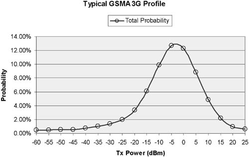
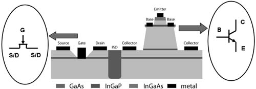
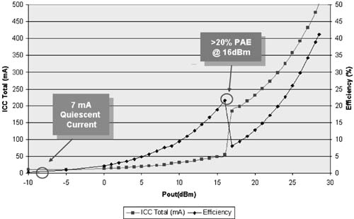
Consumer demand for data and multimedia has prompted telecom operators around the world to upgrade 2G to 3G or above. This trend has sent a very strong signal to mobile device design. This article refers to the address: http:// In addition to providing competitive prices, 3G mobile phones must also transmit higher power, better linearity and better efficiency. Most importantly, 3G phones must have longer talk time because 3G users need to spend more time using their phones. Although battery technology has continued to improve over the past few years, it still lags behind the need for functional expansion. Designers must reduce handset power consumption to meet high power output and longer talk time requirements, which must be achieved by the handset's semiconductor equipment. Since power amplifiers (PAs) are one of the components of today's huge demand, it is meaningful to focus on reducing current consumption through power control. Correspondingly, numerous power control functions can be integrated into the power amplifier module. The integrated power control feature not only emphasizes current power consumption issues, but also provides a more efficient approach to handset design. Chip integration allows handset designers to optimize power management and get longer talk times without the need for separate DC/DC converters and bypass capacitors, while reducing PCB board complexity. Optimize the need for low power output One way to control power consumption in a power amplifier is to increase efficiency over a wide range of output power. This can be achieved by evaluating the handset power distribution curve of the CDG (CDMA Development Group) or the GSMA (GSM Association) in the 3G network to optimize the power amplifier efficiency. Figure 1 shows the power distribution curve of the GSMA used by 3G handset manufacturers. Figure 1 GSMA power distribution curve of 3G network Obviously, the phone works most of the time at low power levels, around the power level of -4dBm. Assuming a circuit loss of approximately 3 dB between the PA and the antenna, the output power of the PA is approximately -1 dBm. At low power levels (below 0dBm), the amplifier consumes mainly quiescent current. - When the output power is 1dBm, the quiescent current of the amplifier is usually about 50mA. By reducing the quiescent current at low power levels and increasing the efficiency of the amplifier, designers can significantly reduce power loss. However, until recently, this has not been feasible. A typical dual-state single-link PA for mobile phones can only be optimized at maximum rated power. This makes the phone very inefficient at low power levels. Of course, by adding an external DC/DC converter and bias voltage control, the efficiency of a single-link power amplifier at low power output can be optimized to achieve increased talk time. But as mentioned above, a DC/DC converter also increases the size and cost of the phone. In addition, this complicates the design because the phone must be calibrated under different analog control conditions. Multi-level optimization of two-way power amplifier ANADIGICS' InGaP-Plus technology solves the power amplifier optimization problem by allowing designers to design amplifiers using multiple gain links. This allows the amplifier to be independently optimized at different power levels. In the general sense of the BiFET process, InGaP-Plus integrates pHEMT (pseudomorphic High Electron Mobility FET) and HBT (Heterojunction Bipolar Transistor) on the same wafer (Figure 2). Figure 2 BiFET process At the same time, high-performance RF switches (pHEMT) coexist on the same crystal. The BiFET process can be used to design amplifiers with multiple gain links, and independent linearity and efficiency optimization for each gain link. InGaP-Plus enables designers to get the best performance from their amplifiers. Originally known as HELP (High Efficiency at Low Power), the technology was designed as a dual-state (high-power and low-power) amplifier. Unlike single-link amplifiers, which have two gain states, the InGaP-Plus amplifier is optimized for high power and low power internally. A single link amplifier cannot do this. Extend your phone's talk time by more than 25% with an internally optimized HELP amplifier. Of course, like a single-link amplifier, you can save more current with an external DC/DC converter. But the extra current savings are not worth it, compared to the increased cost and board area. In recent developments, ANADIGICS used InGaP-Plus BiFETs to design HELP3 amplifiers, with a special three-gain state that allows us to optimize three different power levels. For example, we can optimize high power gain (usually about 28dbm), a moderate power gain of 16dBm, and a low power gain of 7dBm (Figure 3). Figure 3 Typical quiescent current and efficiency curves for a HELP amplifier using a BiFET This is achieved at a low power level of less than 7mA quiescent current in the industry, which is an extraordinary progression compared to the typical 50mA quiescent current in a single link amplifier. Table 1 lists the quiescent current and efficiency comparison data for the latest ANADIGICS WCDMA power amplifier modules made by using special. Table 1: ANADIGICS HELP3 WCDMA Power Amplifier Module Physical, functional, electrical performance improvement In addition to reducing current consumption without the use of an external DC/DC converter, BiFET technology enables manufacturers to integrate other functions, such as integrating LDOs within the amplifier chip, enabling handset manufacturers to reduce board space and further reduce costs. This technology has another advantage: it allows manufacturers to design amplifier modules in smaller areas. As shown in Table 1, ANADIGICS now offers the industry's first 3x3mm single-band and 3x5mm dual-band WCDMA HELP3 power amplifiers HELP3 technology goes hand-in-hand with mobile handset manufacturers that are moving toward low-voltage logic. The new HELP amplifier is designed with a 1.8V logic voltage. These amplifiers will provide longer talk time and further reduce quiescent current by less than 4mA. In addition, ANADIGICS uses BiFET to develop a power amplifier we call ZeroIC, also known as a bypass amplifier. These amplifiers can be completely turned off below a certain power level, so the current consumption is zero, and a switch network is provided. Bypass path to the output of the amplifier module. in conclusion ANADIGICS' innovative InGap-Plus manufacturing is the foundation of HELP power amplifier technology. This fabrication allows for the optimization of high performance RF switches and power amplifiers on the same crystal. ANADIGICS has used this technology to provide the industry's first 3x3 mm single-band and 3x5 mm dual-band WCDMA HELP3 power amplifiers. Vcsel Light Source,Vertical Cavity Surface Emitting Laser,Visible Vcsel,Vcsel 1300Nm AcePhotonics Co.,Ltd. , https://www.acephotonics.com


