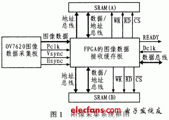
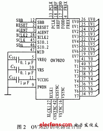
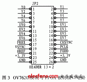
1 Introduction Image acquisition is a prerequisite for image processing. An image capture card is a commonly used image input device that typically occupies one slot of the PC bus. It mainly includes image memory unit, CCD or CMOS camera interface, PC bus interface and so on. Most of the traditional image acquisition cards use the PCI interface. This image acquisition card is suitable for converting analog signals into digital signals by A/D converters, or it is a digital signal itself, and then transmitted to a PC through a PCI interface for image processing. . However, when using an embedded system for image acquisition and processing, an image capture card with a PCI interface is not suitable. To this end, a digital image acquisition module design scheme suitable for embedded systems is proposed here, which realizes image data acquisition, buffering of "ping-pong" mode image data, external interface of image data acquisition module, and ensuring high-speed image acquisition and Continuity. 2 image acquisition system design Figure 1 is a block diagram of an image acquisition system. The system includes an OV7620 image data acquisition board, an image data receiving buffer board of the FPGA, a cache composed of two SRAMs, and a system external interface. OV7620 image data acquisition board mainly completes image data acquisition. Its image data bus, frame image data clock, frame synchronization signal and line synchronization signal are connected with FPGA image data receiving buffer board. FPGA coordinates two SRAM “ping-pong mode†read and write operations. And complete the module's external interface. 2.1 OV7620 image data acquisition board At the heart of the digital image acquisition module is an image sensor. The OV7620 has a built-in 640x480 image array that outputs more than 30 frames per second; it integrates camera functions such as exposure control, gamma, gain, white control, color matrix, color saturation, color control, and window. The device is programmable through the serial SCCB interface and is programmed to output in 8-bit and 16-bit formats. 2.1.1 OV7620 circuit design The system design uses the circuit of OV7620 as shown in Figure 2. Among them, SBB pin jumper is used to set OV7620 to read pin state or I2C mode configuration during reset; UV2 pin is connected to pull-up resistor, select 0V7620 for QVGA working state (320x240); Y3 pin is connected to pull-up Resistor, select OV7620 for RGB data format output: Y1 pin is connected to pull-up resistor, select OV7620 bit progressive scan mode; PWDN pin is grounded, OV7620 can't work in sleep mode; UV0~UV7, Y0~Y7, XCLKl, HSYNC, VSYNC, PCLK, HREF, FODD, FREX are connected to the 26-pin socket, connected to the FPGA, and the 0V7620 is controlled by the FPGA output clock and control signals. When designing the PCB, the analog and digital power supplies, analog ground and digital ground should be separated. The input pin of the power supply is connected to O. 1μF decoupling capacitor and 47μF capacitor to prevent power "surge". The ground is separated from the analog ground and the digital ground, and finally grounded at one point. The crystal oscillator should be placed as close as possible to the device for optimum vibration recovery. 2.1.2 Connection of OV7620 Module to FPGA Board Figure 3 shows the interface circuit between the 0V7620 module and the FPGA board. 3.3 V and GND are powered by the FPGA board. UV0~UV7 and Y0~Y7 are the output bus of image data. VSYNC is the image frame synchronization signal, and HREF is the image. The line sync signal, PCLK is the image data clock on the rising edge of the clock, and the image data is hopped. 2.1.3 MSP430F1121 constitutes the I2C configuration circuit In the design, the MSP430Fll2l MCU is used to configure the OV7620. The MCU downloads the program through the JTAG interface and accesses the 32.768 kHz low-speed crystal oscillator for use by the MCU. The P1.1 and P1.0 ports of the MCU are respectively used as the SCLK and SDA pins of the I2C bus, and each 10 kΩ resistor is pulled up to 3.3 V, which enhances the driving capability of the bus. The internal program of the MCU implements the I2C bus composed of P1.1 and P1.0.
Taillight Wire Harness apply in automotive,motocycle,bus,bike,truck.
Yacenter
has experienced QC to check the products in each process, from developing
samples to bulk, to make sure the best quality of goods. Timely communication
with customers is so important during our cooperation.
If you can't find the exact product you
need in
the pictures,please don't go away.Just contact me freely or send your sample
and drawing to us.We will reply you as soon as possible.
Tail Light Wiring Harness,Trailer Wiring Harness,Trailer Light Wiring Kit,Trailer Light Harness Dongguan YAC Electric Co,. LTD. , https://www.yacentercns.com

