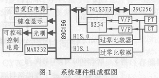
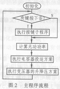
Design of power grid reactive power compensation control system Abstract: This paper introduces a design method of grid reactive power compensation control system composed of single chip system, input/output circuit, keyboard display circuit and communication interface circuit. The system hardware composition and software design of this design method are introduced in detail. The scheme also gives its anti-interference method. Finally, the software design flow chart of the control system is given. Keywords: reactive power compensation thyristor power grid 1 Introduction In the power system, voltage is an important indicator to measure the quality of power. It is the basic task of power system operation adjustment to ensure that the voltage near the user is close to the rated value, and the reactive power has a very close relationship with the voltage. On the one hand, the change of reactive load is much greater than the change of active load when the voltage changes; on the other hand, the voltage fluctuation caused by reactive power is far greater than the change of active load. If the reactive power supply of the power system is sufficient, the need for a reactive balance at a higher level can be met, and the system will also have a higher operating voltage level. Conversely, the lack of reactive power is reflected as a low operating voltage level, which may result in The voltage collapses, thereby damaging the safe operation and operational stability of the power system. Therefore, the reasonable adjustment of voltage and reactive power is of great significance in improving power quality, reducing network loss, stability and safety of operating grid operation. The method of adjusting the reactive power is to adjust the size of the grid compensation capacitor according to the size of the reactive power. Because the reactive power transmission loss is large, it is not suitable for long-distance transmission. Therefore, the reactive power required for the load should be as close as possible to the local supply. 2 system hardware design The hardware component block diagram of the reactive power compensation control system of this power grid is shown in Figure 1. It mainly consists of a single-chip system (self-reset circuit composed of 80196 MCU, 74LS373, FLASH MEMERY 29C256), keyboard display circuit, input circuit, output circuit and communication interface circuit MAX232. 2.1 single chip system The core part of the system is an 80196KB microprocessor, and the 80196KB is a MCS-96 series 16-bit processor. Its powerful functions, rich resources and high efficiency lay the foundation for the fast and real-time operation of the whole system. 2.2 input circuit The input circuit is composed of a phase difference detecting circuit of voltage and current and a voltage and current effective value detecting circuit. The voltage and current phase difference detection circuit is composed of PT (voltage transformer), CT (current transformer) and zero-crossing detection circuit. The PT can be used to convert high voltage on the grid into a low voltage signal and convert it into a square wave signal after zero crossing detection. CT converts the current on the grid into a voltage signal, which is also converted into a square wave after zero-crossing detection. The CPU calculates the time difference Δt by detecting the rising edge of this square wave, and then compares it with the measured period T to obtain the phase difference φ, that is: φ=2πΔt/T The voltage and current RMS detection circuit is composed of a PT, a CT, a V/F circuit, and a counter 8254. The V/F circuit uses an AC V/F circuit. This V/F circuit has the following advantages: ◠Speed ​​up the tracking of measured changes. ◠Reduced intermediate links, thus reducing errors and sources of interference. ◠Simplified installation and wiring. ◠Reduced hardware investment in the transmitter. ◠You can make a reasonable choice between sampling speed and accuracy through software. The 8254 chip is a counter. Through its timing counting, a series of instantaneous values ​​of voltage and current signals can be obtained, and then the software and a series of algorithms are used to obtain the effective values ​​of voltage and current. Common algorithms include full-wave Fourier algorithm, half-wave Fourier algorithm, two-point product algorithm, and derivative algorithm. The system uses the full-wave Fourier algorithm, because the algorithm is more accurate than other algorithms, so the required data window is longer and the calculation process is slower. Therefore, considering the speed and accuracy of the system, the author chooses the precision. High algorithm. The idea of ​​the full-wave Fourier algorithm is based on the Fourier series, because the voltage and current signals are a periodic function and can be decomposed into infinite series of DC components, fundamental and subharmonics. which is: 2.3 output circuit After the output circuit is isolated by the optocoupler, the thyristor control circuit can be driven to control the on/off operation of the thyristor, that is, whether the capacitor is used. In addition, when voltage regulation is required, the boost and buck of the transformer can also be controlled. 2.4 Communication interface The communication interface of the control system adopts 232 interface, and the interface circuit is designed by MAX232 special 232 interface circuit chip produced by MAXIM. The core sleep has the characteristics of simple use and reliable performance. 3 software design The system software is written in PLM96 language, and its main program block diagram is shown in Figure 2. At the same time, the program also opened three interrupts: HIS interrupt, timer interrupt and serial interrupt. The HIS interrupt is used to accurately record the time of the rising edge of the voltage and current square waves, and provides real-time values ​​for calculating the phase difference for the main program in time. The timer interrupt is used to periodically sample the voltage and current; the serial interrupt is used when the system is connected to the network. Implement communication functions. In order to make these three interrupts do not affect each other, each interrupt subroutine should be as short as possible, and the nesting of each interrupt can also be considered. The system software opens the timer interrupt and HIS interrupt in the serial interrupt. The real-time requirements of these two interrupts are relatively high and the interruption time is also very short. Through the opening of three kinds of interrupts, the real-time performance of various parameters of the system can be improved, and the main program is also simpler and more efficient. 4 Conclusion Since the system was put into use, it has been running stably, saving a lot of expenses for manufacturers and users, thus increasing economic benefits and being well received by users and manufacturers.
Laptop power adapter charger for Asus:
Our service:
Stable output and high charging efficiency.
Elegant outlook design as original one, touch smoothly and comfortable.
Original charger is good, but as a replacement, our product has more reasonable price when your original charger is broken.
And, the market of the replacement adapters becomes bigger and bigger. People would rather buy a copy one then the original because of the price.
But at the same time, people worry about that they will buy something defective. So the problem comes, how to buy a good quality one with a good price?
As a professional power adapter manufacturer, we have excellent R&D team, skilled staffs and responsible after-sale service. All your benefits can be under protected after you buy products for our company.
Our certificates :ISO9001:2008 & ISO14001:2004 , CCC , CE , FCC , ROHS.
All our products has 1 year warranty. In other words, if you get the dad products which are not damaged physically from us in one year, we will replace you the new one or the whole bulk order.
Asus Adapter,Adapter For Asus,Laptop Adapter For Asus ,Power Supply For Asus Shenzhen Waweis Technology Co., Ltd. , https://www.huaweishiadapter.com

The base current can be obtained: 
The system uses a 13-point algorithm, ie N=13. 
Laptop Model
Power Adapter
K42F K42JB K42JK K42JR K42JV K52f A52f A42 X52f A52 A52f A52J
19v 3.42a, 5525
K60IJ K50IJ K50I K60I
19v 4.74a, 5525