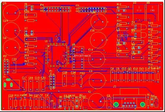
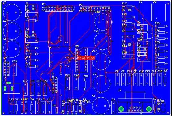
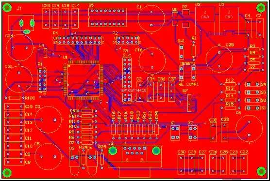
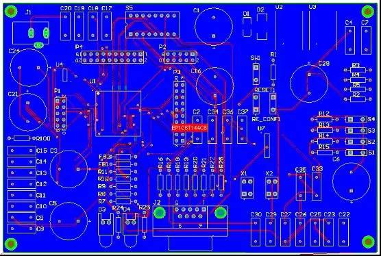
Here, I will first take a look at the "horrible" PCB on which I originally drew this development board. Top Layer as shown: Bottom Layer as shown: When I first painted it, I wanted to finish it quickly and sloppy. However, after all the wiring was finished, I found that there were too many mistakes. I think the most important mistake was to start from the beginning. Without paying attention to the layout of the various components of the entire system, this led to the occurrence of "catastrophe", and later wiring was very difficult. It is easy for everyone to see in the picture above that the length of the wiring is very long. In fact, this is also a very serious mistake, especially for high-speed signal lines. The wires used for input and output should be as short as possible, and they should not be paralleled as long as possible, except for differential lines. We know that in fact, each component will have pin inductance. From the pin leads of the chip to the leads of the resistors, capacitors, and inductors, each line and trace has parasitic capacitance and inductance. They directly affect the impedance of the wire. And sensitive to high frequencies. In general, the wires exhibit resistive characteristics at low frequencies. According to the theory of RF circuits, the wires exhibit inductive characteristics at high frequencies. The board I draw is 25 MHz, so this factor can be ambiguous. However, in order to prevent unnecessary troubles, it is better to take 1/20 of the wavelength less than 150MHz when taking high-frequency signal lines, so as to avoid unexpected interference sources on the board, because when the signal frequency exceeds 150MHz, the PCB goes The line is equivalent to "becoming" an effective antenna! We must also pay attention to the differential signal traces. It is very important that the differential signal lines on the board must be as long as possible, and for signal rates above 100 MHz, the high-speed connector with impedance control must also be used. I don't need to think about this when I draw this board, but I'm still wary of it. By the way, I'll mention it here. Hey, if you have such a high frequency in the future, you have to think about it, otherwise it will cause EMI problems. Oh. Do not know if you have not found that in the above I painted the PCB actually contains a very good advantage, that is, the entire board has very few vias! Everyone should know that we should use as few or no vias as possible when wiring, because this will bring more bus model inductances, which may degrade the signal quality and even cause EMI problems. That can be more troublesome. Afterwards, I painted a few times again, and then took a picture and looked at it. Top Layer as shown: Bottom Layer as shown: The feeling is still better than the picture drawn in the first pass, but it is certainly possible to draw better, but just think that the current level of this level, and later practice slowly!
An electric slip ring is a rotary electrical connector. It allows uninterrupted power or signal transfer between two stationary points. It is also known as an electric Rotary Joint, power swivel, or electrical rotary joint. Electric slip rings are usually composed of a metal ring with several brush contacts on the inner circumference. And there are one or more pairs of contacts for power or signals on the outer circumference. The metal ring can be rigid or flexible, depending on the application.
An electric slip ring is an electromechanical device that allows the transmission of electrical power and signals from a stationary to a rotating structure. It consists of an electrically conductive rotating disc or ring, with a number of electrical contacts (or "slots") on its surface. The contacts are connected to external circuits, enabling the passage of power and/or data from the stationary to the rotating structure. Slip rings are also used in generators, where they allow the passage of current from the rotor to the stator.
A flat disc electrical slip ring is one kind of electric slip ring, it has many advantages: simple construction, small size, low cost, easy installation, and maintenance. It is widely used in various fields such as machine tools, textile machinery, printing machinery, packaging machinery, medical equipment, and aerospace equipment.
A 360-degree rotating Conductive Slip Ring is also called a hollow shaft slip ring or hollow conduct. It has an opening in the center that allows a shaft to pass through, making it ideal for rotating applications. Slip rings are often used in medical equipment, robotics, and manufacturing assemblies where rotation is required. This type of slip ring can handle large currents and voltages while providing a continuous electrical connection.
Electric Slip Ring,Slip Rings In Generator,Flat Disc Electrical Slip Ring,Slip Ring Electric Motor Dongguan Oubaibo Technology Co., Ltd. , https://www.sliprobs.com


