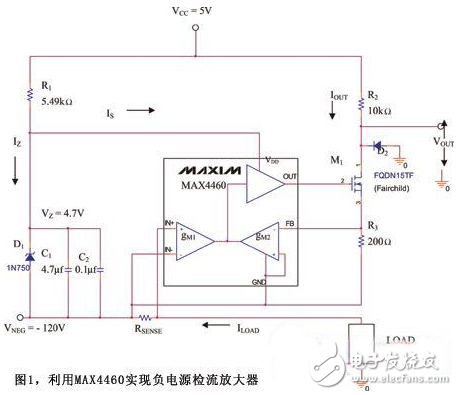
High-side current-sense amplifiers are typically used when monitoring the current of a positive supply. However, for ISDN, telecom power supplies, a current-sense amplifier operating at a negative supply is usually required. This article describes a method for designing a negative-voltage current-sense amplifier using the MAX4460 single-supply instrumentation amplifier. The circuit shown in Figure 1 provides a block diagram of a negative supply current sense using a MAX4460 or MAX4208 instrumentation amplifier with some discrete components. Zener diode D1 provides overvoltage protection for the instrumentation amplifier with sufficient supply voltage. The monitored current flows into the negative supply through the current-sense resistor RSENSE. The instrumentation amplifier must be powered from a single supply and have ground potential detection capability. The output of the MAX4460 provides the gate drive for MOSFET M1, and the negative feedback loop ensures that the voltage across resistor R3 is equal to the voltage across the RSENSE, VSENSE. Correspondingly, a current proportional to the load current is established by R3: IOUT = (ILOAD &TImes; RSENSE)/R3 = VSENSE/R3 (1) The choice of R2 is to ensure that the output voltage is within the voltage range required by the latter circuit (usually the ADC). The drain-source breakdown voltage needs to be higher than the sum of the two supply voltages (here +125V). If the ADC is not a high-impedance input, an additional buffer amplifier is required at the output VOUT. If the sense current rises above the rated value in the event of a fault, the input voltage becomes a negative value. Diode D2 limits the negative voltage at the output to the voltage drop across a diode, providing protection for the downstream ADC. The above design can be easily used for current detection of high voltage and negative power supplies. Select -120V as the negative power supply, follow the steps below to get the current sense amplifier under different power supply voltages. The Zener is biased to operate at a lower operating point of the transmission characteristic (e.g., in the region where it enters reverse breakdown), which eliminates PSRR errors. The Zener voltage is not very stable near the breakdown voltage. The bias point is typically set at 25% of the maximum current specified by the rated power. This bias point has a lower dynamic resistance and does not consume a lot of power. Resistor R1 is selected as follows to operate the circuit at the desired bias point. IR1 = ( VCC + |VNEG| - VZ )/R1 = IS + IZ (2) Where: VCC is the positive supply voltage, VZ is the Zener tube stable voltage, |VNEG| is the absolute value of the negative supply voltage, IS is the supply current of the MAX4460, and IZ is the current flowing through the Zener. R1 must have an appropriate power rating to withstand the high voltages at both ends. It is also possible to use strings and combinations to reduce the requirements for the rated power of the resistor. When selecting an N-channel MOSFET or JFET, ensure that the rated breakdown voltage between the drain and source is greater than |VNEG| + VCC. This is very important for situations where the negative pressure is high. When selecting RSENSE, it is necessary to ensure the full-scale voltage, and the detection voltage across RSENSE is less than or equal to 100mV. The choice of R3 is flexible and is mainly affected by the following two conditions: (1) When R3 is decreased, it can be seen from Equation 1 that power consumption will increase for a fixed gain. (2) The thermal noise and leakage current of the FET determine the upper limit of the choice of R3. Select the resistance ratio of R2 and R3 to be equal to the voltage gain of the current-sense amplifier. The output voltage is: VOUT = VCC - IOUT &TImes; R2 (3) From Equation 1 and Equation 3, you can get: VOUT=VCC-(VSENSE&TImes;R2/R3) For VSENSE: Voltage gain, Av = -R2/R3 (4) A negative sign indicates that the output voltage is inversely related to the input sense voltage. From Equation 4, R2 can be solved. The following typical parameters are used for the derivation of the current-sense amplifier: Input offset voltage = (5 - 4.9831) / 49.942 = 338mV Gain = -49.942 This article describes the implementation of a negative supply current sense with the precision instrumentation amplifier MAX4460. The circuit can be redesigned according to the above design steps for monitoring different negative voltage sources.
2D Wireless Scanner Product Features: 1. Excellent performance, can collect barcodes under almost any conditions 2. Satisfy the 24-hour uninterrupted scanning power, independent power display 3. Exclusive Wi-Fi friendly mode eliminates Bluetooth interference
ShengXiaoBang is the Barcode scanner and Printer manufacturer in China.
with over 6years export experience that we know the quality is our soul.
Many clients re-order to us for our stable quality and competitive price.
please contact us for more information and you will get what you really want.
2D Wireless Scanner ,Wireless 2D Barcode Reader,Cordless 2D Barcode Scanner,Scanner 2D Wireless ShengXiaoBang(GZ) Material Union Technology Co.Ltd , https://www.sxbgz.com