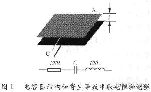
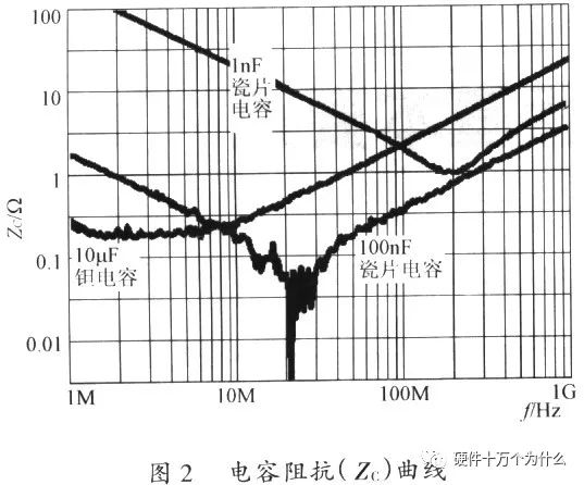
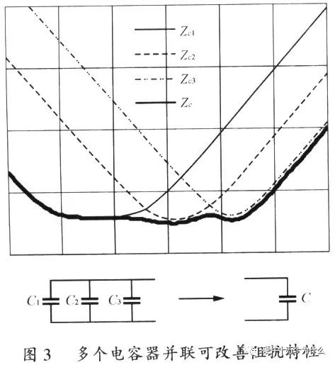
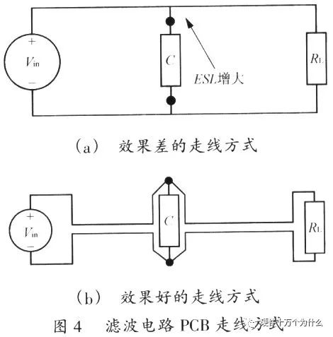
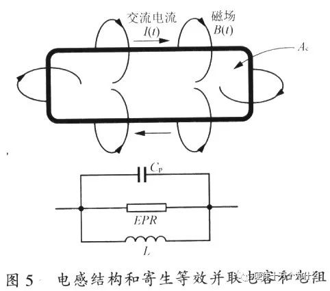
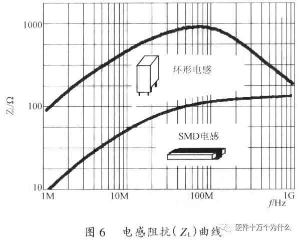
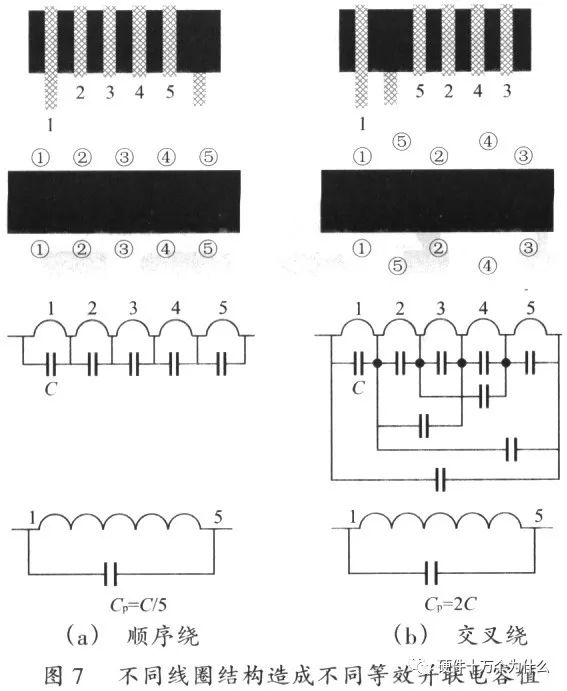
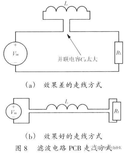
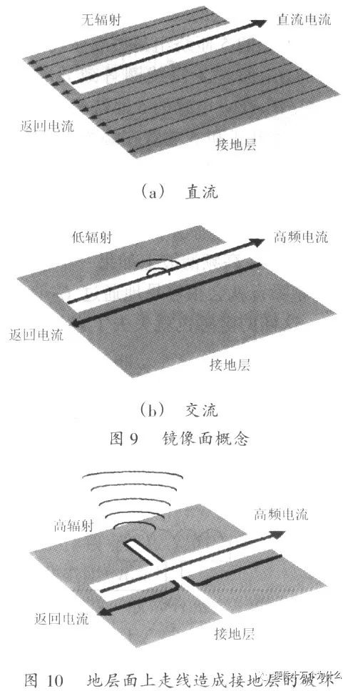
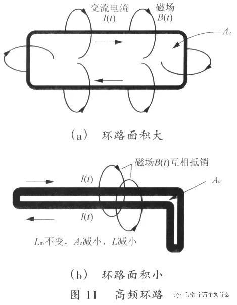
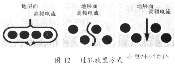
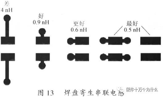
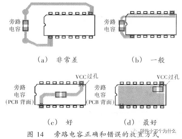
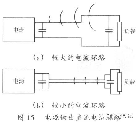
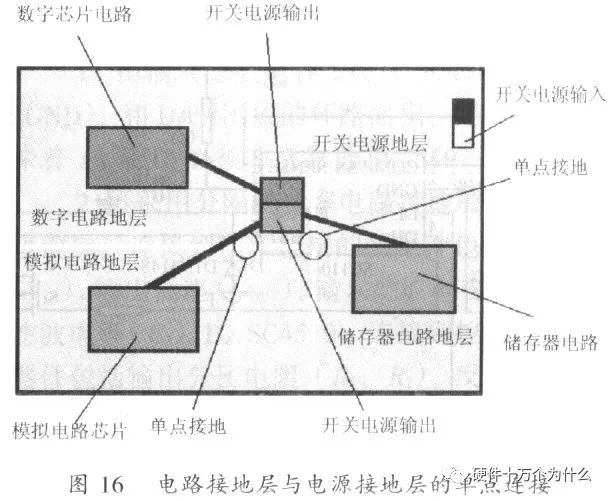
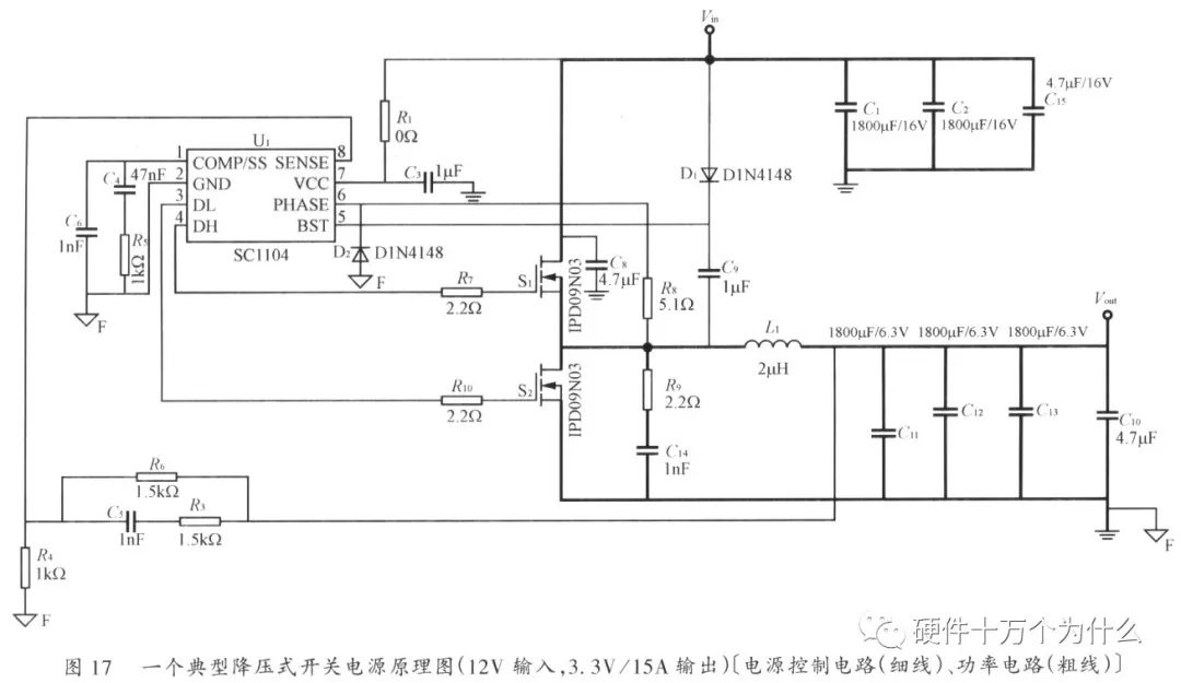
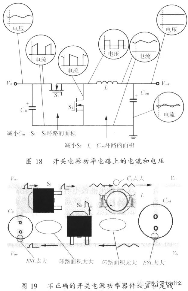
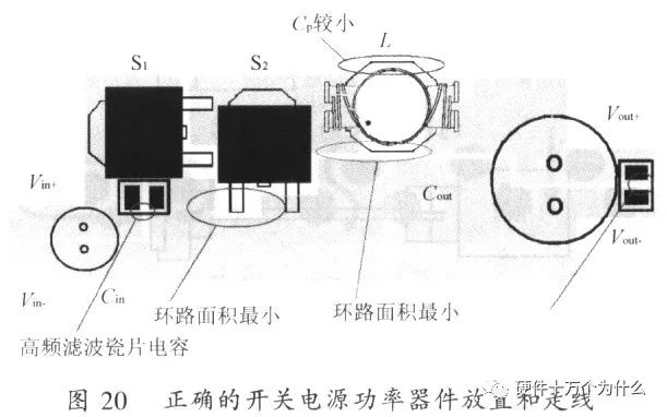
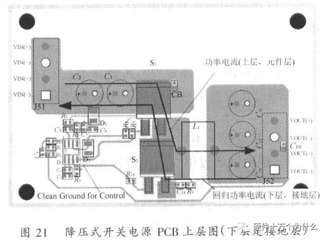
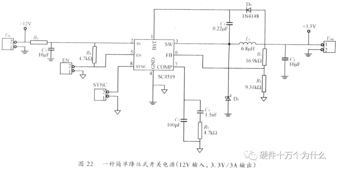
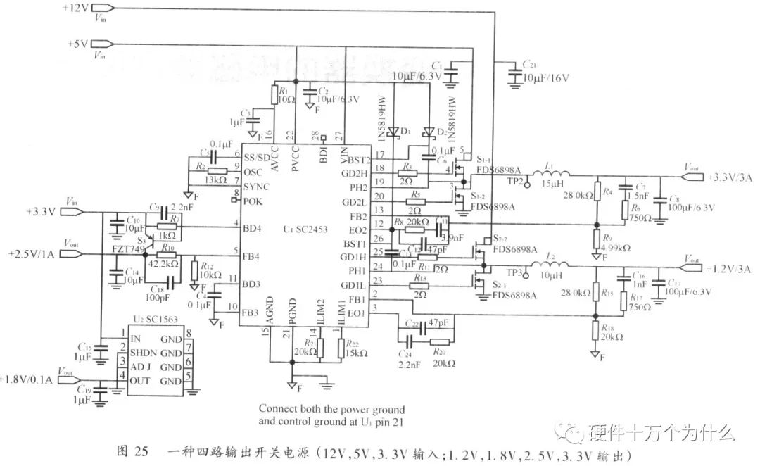
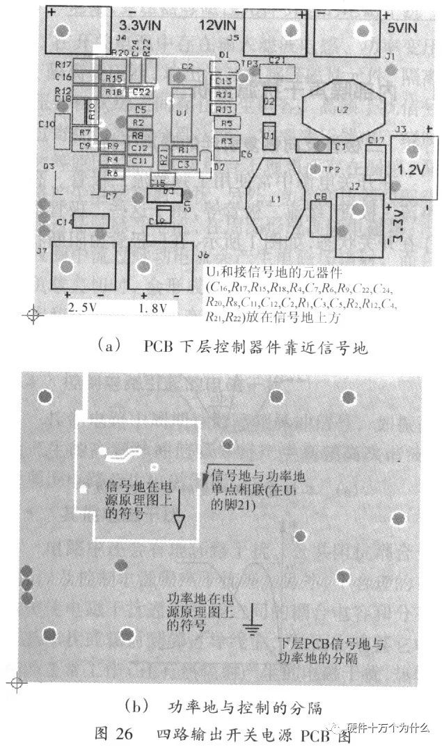
Abstract: Switching power supply PCB layout is an important process in the development of power supply products. In many cases, a power supply that is perfectly designed on paper may not work properly during initial commissioning, because there are many problems with the PCB layout of the power supply. The basic points of PCB layout for switching power supplies are discussed in detail, and some practical PCB layout examples are described. 0 Preface In order to adapt to the rapid replacement of electronic products, product design engineers are more inclined to choose AC / DC adapters that are easily available on the market and install multiple sets of DC power supplies directly on the system's circuit board. Because the electromagnetic interference generated by the switching power supply will affect the normal operation of its electronic products, the correct power supply PCB layout becomes very important. Switching power supply PCB layout is completely different from digital circuit PCB layout. In digital circuit layout, many digital chips can be automatically arranged by PCB software, and the connecting lines between the chips can be automatically connected by PCB software. The switching power supply discharged by automatic typesetting will definitely not work normally. Therefore, no one needs to have a certain understanding of the basic rules of switching power supply PCB layout and the working principle of switching power supply. 1 Basic points of PCB layout for switching power supply l.1 Capacitor high frequency filtering characteristics Figure 1 is the basic structure of the capacitor and the high-frequency equivalent model. The basic formula of capacitance is Equation (1) shows that reducing the distance between the capacitor plates (d) and increasing the cross-sectional area of ​​the plates (A) will increase the capacitance of the capacitor. Capacitors usually have two parasitic parameters, equivalent series resistance (ESR) and equivalent series inductance (ESL). Figure 2 is the impedance (Zc) of the capacitor at different operating frequencies. The resonance frequency (fo) of a capacitor can be obtained from its own capacitance (C) and equivalent series inductance (LESL), namely When the operating frequency of a capacitor is below fo, its impedance decreases with increasing frequency, ie When the operating frequency of the capacitor is above fo, its impedance will increase as the frequency increases, ie When the operating frequency of the capacitor is close to fo, the capacitance impedance is equal to its equivalent series resistance (RESR). Electrolytic capacitors generally have a large capacitance and a large equivalent series inductance. Due to its low resonance frequency, it can only be used for low-frequency filtering. Tantalum capacitors generally have a larger capacitance and a smaller equivalent series inductance, so its resonant frequency will be higher than that of electrolytic capacitors, and can be used in high-frequency filtering. Ceramic capacitor capacitance and equivalent series inductance are generally very small, so its resonance frequency is much higher than electrolytic capacitors and tantalum capacitors, so it can be used in high-frequency filtering and bypass circuits. Since the resonant frequency of small capacitance ceramic capacitors will be higher than that of large capacitance ceramic capacitors, it is not possible to use ceramic capacitors with excessively high capacitance values ​​when selecting bypass capacitors. In order to improve the high-frequency characteristics of the capacitor, multiple capacitors with different characteristics can be used in parallel. Figure 3 shows the effect of impedance improvement after multiple capacitors with different characteristics are connected in parallel. The basic points of power supply layout 1 The capacitance of the bypass ceramic capacitor should not be too large, and its parasitic series induction is as small as possible. Multiple capacitors in parallel can improve the high-frequency impedance characteristics of the capacitor. Figure 4 shows the different traces of input power (Vin) to load (RL) on a PCB. In order to reduce the ESL of the filter capacitor (C), the lead length should be as short as possible; and Vin. The traces from positive to RL and negative to R1 should be as close as possible. 1.2 High-frequency filter characteristics of inductance The current loop in Figure 5 is similar to the inductance of a one-turn coil. The electromagnetic field R (t) generated by the high-frequency alternating current will surround the outside and inside of this loop. If the high-frequency current loop area (Ac) is large, a large amount of electromagnetic interference will be generated inside and outside this loop. The basic formula of inductance is From equation (5), we can see that reducing the loop area (Ac) and increasing the loop circumference (lm) can reduce L. Inductance usually has two parasitic parameters, equivalent parallel resistance (EPR) and equivalent parallel capacitance (Cp). Figure 6 shows the impedance (ZL) of the inductor at different operating frequencies. The resonance frequency (fo) can be obtained from the inductance value of the inductor itself (L) and its equivalent parallel capacitance value (Cp), namely When the operating frequency of an inductor is below fo, the impedance of the inductor increases with increasing frequency, ie When the operating frequency of the inductor is above fo, the impedance of the inductor decreases with increasing frequency, ie When the operating frequency of the inductor is close to fo, the impedance of the inductor is equal to its equivalent parallel resistance (REPR). The Cp of the inductor in the switching power supply should be controlled as small as possible. At the same time, it must be noted that the inductance of the same inductance will produce different Cp values ​​due to the different coil structure. Figure 7 shows the different Cp values ​​for the same inductance with two different coil configurations. Fig. 7 (a) The 5-turn winding of the inductor is wound in order. The Cp value of this coil structure is 1/5 of the equivalent parallel capacitance value (C) of the 1-turn coil. Fig. 7 (b) The 5-turn winding of the inductor is wound in a cross order. Among them, windings 4 and 5 are placed between windings 1, 2, and 3, while windings 1 and 5 are very close. The Cp produced by this coil structure is twice the C value of a 1-turn coil. It can be seen that the Cp values ​​of the two inductors with the same inductance actually differ by several times. In high frequency filtering, if the Cp value of an inductor is too large, high frequency noise will be easily coupled directly to the load through Cp. Such an inductor will also lose its high-frequency filtering function. Figure 8 shows the different routing of Vin through L to the load (RL) on a PCB. In order to reduce the Cp of the inductor, the two pins of the inductor should be as far away as possible. The traces from Vin positive to RL and Vin negative to RL should be as close as possible. The basic points of power supply layout 2 The parasitic parallel capacitance of the inductor should be as small as possible. 1.3 Mirror surface The concept of mirror surface in electromagnetic theory will be of great help for designers to master the PCB layout of switching power supplies. Fig. 9 is the basic concept of the mirror surface. Figure 9 (a) is the scenario when DC current flows over a ground plane. At this time, the return DC current on the stratum is very evenly distributed throughout the stratum. Figure 9 (h) shows the scenario when high-frequency current flows over the same stratum. At this time, the return AC current on the stratum can only flow in the middle of the stratum and there is no current on both sides of the stratum. One day. Understanding the concept of mirror plane, we can easily see the problem of routing on the ground plane in Figure 10. The ground plane (Ground Plane), no juice personnel should try to avoid placing any power or signal traces on the ground plane. Once the trace on the ground layer destroys the entire high-frequency loop, the circuit will produce strong electromagnetic radiation and destroy the normal operation of the surrounding electronic devices. Basic points for power supply layout 3 Avoid placing any power or signal traces on the ground. 1.4 High frequency loop There are many high-frequency loops composed of power devices in the switching power supply. If the △ loop is not good, it will have a great impact on the normal operation of the power supply. In order to reduce the electromagnetic wave noise generated by the high-frequency loop, the area of ​​the loop should be controlled to be very small. As shown in Figure l1 (a), the area of ​​the high-frequency current loop is large, and strong electromagnetic interference will be generated inside and outside the loop. For the same high-frequency current, when the loop area is designed to be very small, as shown in Figure 11 (b), the electromagnetic fields inside and outside the loop cancel each other out, and the entire circuit becomes very quiet. Basic points of power supply layout 4 The area of ​​the high-frequency loop should be reduced as much as possible. 1.5 Via and pad placement Many designers like to place many vias (VIAS) on the multilayer PCB. However, it is necessary to avoid placing too much on the same path of high-frequency current return. Otherwise, high-frequency current traces on the ground will be destroyed. If you must place some vias on the high-frequency current path, you can leave a space between the vias for high-frequency current to pass smoothly. Figure 12 shows the via placement method. Basic points of power supply layout 5 The placement of vias should not disrupt the flow of high-frequency currents on the ground. Designers should also note that different pad shapes will produce different series inductances. Figure 13 shows the series inductance values ​​for several pad shapes. The placement of the bypass capacitor (Decouple) should also consider its series inductance value. The bypass capacitor must be a ceramic capacitor with low impedance and low ESL. But if a high-quality ceramic capacitor is placed on the PCB in a wrong way, its high-frequency filtering function will disappear. Figure 14 shows the correct and incorrect placement of bypass capacitors. 1.6 Power DC output The load of many switching power supplies is far from the output port of the power supply. In order to prevent the output traces from being disturbed by the electromagnetic interference generated by the power supply itself or the surrounding electronic devices, the output power traces must be very close as shown in Figure 15 (b) to minimize the area of ​​the output current loop. l.7 Separation of strata on the system board The new generation of electronic product system board seven will have analog circuits, digital circuits, and switching power supply circuits. In order to reduce the impact of power supply noise on sensitive analog and digital circuits, it is usually necessary to separate the ground layers of different circuits. If a multilayer PCB is used, the ground layers of different circuits can be separated by different PCB layers. If the entire product has only one ground layer, it must be separated in a single layer as shown in Figure 16. Whether the ground layer is separated on a multilayer PCB or the single layer PCB, the ground layers of different circuits should be connected to the ground layer of the switching power supply through a single point. Basic points of power supply layout 6 Seven different circuits on the system board require different ground layers. The ground layers of different circuits are connected to the power ground layer through a single point. 2 PCB power supply layout example Schematic diagram of pressure switching power supply. The designer should be able to distinguish the components in the power circuit and the components in the control signal circuit on this circuit diagram. If the designer treats all the components in the power supply as components in the digital circuit, the problem will be quite serious. Usually first need to know the path of the high-frequency current of the power supply, and distinguish the small signal control circuit and the power circuit components and their wiring. Generally speaking, the power circuit of the power supply mainly includes an input filter capacitor, an output filter capacitor, a filter inductor, and upper and lower power field effect transistors. The control circuit mainly includes a PWM control chip, a bypass capacitor, a bootstrap circuit, a feedback voltage divider resistor, and a feedback compensation circuit. 2.l PCB layout of power supply circuit The correct placement and routing of power devices on the PCB will determine whether the entire power supply is working properly. The designer must first have a certain understanding of the voltage and current waveforms on the power device of the switching power supply. Figure 18 shows the current and voltage waveforms of the power circuit components of a step-down switching power supply. Since the current flowing through the input filter capacitor (Cin), the upper field effect tube (S1) and the F field effect tube (S2) is an alternating current with a high frequency and a high peak value, so Cin-S1-S2 The loop area formed should be minimized. At the same time, the loop area composed of S2, L and the output filter capacitor (Cout) should also be minimized. If the designer does not make the power circuit PCB according to the points described in this article, it is likely to produce the power PCB shown in the net 19. There are many errors in the PCB layout of Figure 19: First, because Cin has a large ESL, The high-frequency filtering capability of Cin basically disappears; second, the area of ​​the Cin-S1-S2 and S1-LCout loops is too large, and the generated electromagnetic noise will cause much disturbance to the power supply itself and the surrounding circuits; third, L The pads are too close together, which causes Cp to be too large and reduces its high-frequency filtering function. Fourth, the lead of the Cout pad is too long, which causes the FSL to be too large and lose the high-frequency filtering line. The area of ​​the Cin-S1-S2 and S2-L-Cout loops has been controlled to a minimum. The connection point between the source of S1, the drain of S2 and L is a whole copper pad. Since the voltage at this connection point is high frequency, S1, S2, and L need to be very close together. Although there is no high-peak high-frequency current on the trace between L and Cout, the wider trace can reduce the loss of DC impedance and improve the efficiency of the power supply. If the cost permits, the power supply can use a double-sided PCB with a ground plane, but it must be careful to avoid power and signal lines on the ground layer. A ceramic capacitor is added to the input and output ports of the power supply to improve the high-frequency filtering performance of the power supply. 2.2 PCB layout of power control circuit PCB layout of power control circuit is also very important. Unreasonable layout will cause the output voltage of the power supply to drift and oscillate. The control circuit should be placed on the side of the power circuit, and must not be placed in the middle of the high-frequency AC loop. The bypass capacitor should be as close as possible to the Vcc and ground pin (GND) of the chip. The feedback resistor divider is also best placed near the chip. The loop that the chip drives to the field effect tube should be as short as possible. Basic points of power supply layout 7 The drive circuit loop from the control chip to the upper and lower field effect transistors should be as short as possible. 2.3 PCB power supply layout example 1 FIG. 21 is a wiring diagram of the component surface of the PCB of FIG. 17. A low-cost PWM controller (Semtech model SCIIO4A) is used in this power supply. The lower layer of the PCB is a complete ground plane. There is no separation between this PCB power ground plane and the control ground plane. It can be seen that the power circuit of the power supply passes from the input socket (upper left end of the PCB) through the input filter capacitors (C1, C2,), S1, S2, L1, and output filter capacitors (C10, C11, C12, C13) all the way to the output socket (Bottom right of PCB). SCll04A is placed on the lower left end of the PCB. Because the power circuit current does not pass through the control circuit on the ground layer, there is no need to separate the control circuit ground layer from the power circuit ground layer. If the input socket is placed on the lower left end of the PCB, then the power circuit current on the ground layer will directly pass through the control circuit, then it is necessary to separate the two. 2.4 PCB power supply layout example 2 Figure 22 is another step-down switching power supply, the power supply can convert 12V input voltage into 3.3V output voltage, the output current can reach 3A. An integrated power controller (Semtech model SC4519) is used on this power supply. This controller integrates a power tube in the power controller chip. Such a power supply is very simple, especially suitable for consumer electronic products such as portable DVD players, ADSL, set-top boxes and so on. As with the previous example, for this simple switching power supply, the following points should also be noted when PCB layout. 1) The loop area formed by the input filter capacitor (C3), the ground pin (GND) of SC4519, and D2 must be small. This means that C3 and D2 must be very close to SC4519. 2) Separate power circuit ground layer and control circuit ground layer can be used. Components connected to the power ground include input socket (VIN), output socket (VOUT), input filter capacitor (C3), output filter capacitor (C2), D2, SC4519. Components connected to the control ground include output voltage divider resistors (R1, R2), feedback compensation circuits (R3, C4, C3,), enable socket (EN), and synchronization socket (SYNC). 3) Add a via in the vicinity of the SC4519 ground pin to connect the power circuit ground layer to the control signal circuit ground layer in a single point. Figure 23 is a layout diagram of the upper layer of the power PCB. For the convenience of the reader, the power ground layer and the control signal ground layer are represented by different colors. Here the input socket is placed above the PCB, and the output socket is placed below the PCB. The filter inductor (L1) is placed on the left side of the PCB and close to the power ground plane, while the feedback compensation circuit (R3, C4, C5) sensitive to noise is placed on the right side of the PCB and close to the control signal ground plane. D2 is very close to feet 3 and 4 of SC4519. Fig. 24 is a layout diagram of the lower layer of the power PCB. The input filter capacitor (C3) is placed under the PCB and very close to the SC4519 and power ground plane. 2.5 Switching power supply PCB layout example 3 Finally, the main points of PCB layout for a multi-output switching power supply are discussed. This power supply has 3 sets of input voltage (12V, 5V and 3.3V) and 4 sets of output voltage (3.3v, 2.6V, 1.8V, 1.2V). The power supply is used, an integrated multi-way switch controller (Serotech model SC2453). The SC2453 provides a wide input voltage range of 4.5V to 30V, two synchronous buck converters with switching frequencies up to 700kHz and output currents up to 15A, and output voltages down to 0.5V. It also provides a dedicated adjustable positive pressure linear regulator and a dedicated adjustable negative pressure linear regulator. The TSSOP-28 package reduces the required circuit board area. Two out-of-phase buck converters can reduce input current ripple. Figure 25 is a schematic diagram of such a multi-channel switching power supply. Among them, 3.3V output is generated by 5V input, 1.2V output is generated by 12V input, and 2.6V and 1.8V output are generated by 3.3V input. Since all components on the power supply must be placed on a PCB with a small area, the power ground and control signal ground of the power supply must be separated. With reference to the points discussed in the previous sections, first distinguish the components connected to the power ground plane from the components connected to the control signal ground plane in Figure 25, and then place the control signal components on the signal ground plane near the SC2453 control The signal ground and the power ground are connected by a single point. This connection point is usually selected at the ground pin of the control chip (pin 21 in SC2453). Figure 26 describes this power supply layout in detail. Basic points of power supply layout 8 The components under the switching power supply circuit and the control signal circuit need to be connected to different ground layers. These two ground layers are generally connected through a single point. 3 Conclusion 8 main points of switching power supply PCB layout: 1) The capacitance of the bypass ceramic chip capacitor cannot be too large, and its parasitic series electrical induction is as small as possible. Multiple capacitors in parallel can improve the impedance characteristics of the capacitor; 2) The parasitic parallel capacitance of the inductor should be as small as possible, the farther the distance between the inductance pin pads is, the better; 3) Avoid placing any power or signal traces on the ground layer; 4) The area of ​​the high-frequency loop should be reduced as much as possible; 5) Small via placement should destroy the path of high-frequency current on the ground; 6) A small circuit on the system board needs different ground layers. The ground layer of the small circuit is connected to the power ground layer through a single point; 7) The drive circuit loop from the control chip to the upper and lower field effect transistors should be as short as possible; 8) The switching power supply power circuit and control signal circuit components need to be connected to the same ground layer. These two ground layers are generally connected through a single point. Silent Type Diesel Generator,Soundproof Diesel Generator,Diesel Generator Set,Pump Generator Jiangsu Vantek Power Machinery Co., Ltd , https://www.vantekpower.com