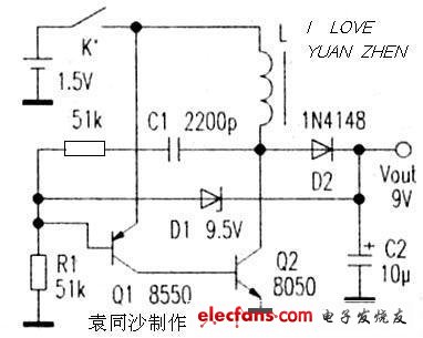
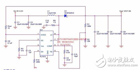
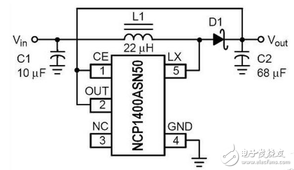
C1 is the role of positive feedback. When Q2 turns on, the positive feedback of C1 causes Q2 to quickly enter the saturation region. Then C1 discharges and reverses charging. As the base potential of Q1 increases, the base current of Q2 also decreases, and the current on L1 rises continuously. When it reaches a large enough Q2 to exit saturation, Q2 collector potential Raise, the positive feedback of C1 is given to the base of Q1 to increase the potential, so that Q1, Q2 will immediately return to the cut-off area. Q1 is turned on again, and it is necessary to recharge the R1 and C1 to lower the base potential of Q1. It takes a long time, so the charging time of the circuit L1 is usually much longer than the discharge (including waiting for recharging). Time. When D1 is connected, the output voltage is too high, which will affect the charging and discharging of C1, resulting in shorter on-time of Q1 and Q2 and longer waiting time after discharge. As can be seen from the above analysis, the operating frequency of this circuit is related to both R1 and C1. It is also affected by L1, but it has little effect. The driving ability of this circuit is related to the value of R1, L1 and the amplification factor of Q1 and Q2. This circuit is easy to start, and the conditions for no vibration are: R1 is relatively small. After Q1 and Q2 are turned on, C1 reverse charging is completed, and Q1 current reaches the minimum value. If Q2 is still in the saturation region (the internal resistance of L1 limits the collector current of Q2 to rise further), this It consumes a lot of power and the circuit stops. 3.7V to 12V1.5A, 3.7V boost 12V1.5A circuit diagram, non-synchronous rectification boost typical circuit, external Schottky diode. The periphery is simple. Overcurrent protection (OCP) detects the MOS current between LX and GND, which is the peak current of the inductor. Triggering the overcurrent will reduce the duty cycle, and the inductor current will also decrease. When the duty cycle is above 50%, the duty cycle will be reduced. OCP, in order to make the PWM stabilize the square wave, the IC internally performs slope compensation. The larger the duty ratio, the lower the OCP. The OCP is adjusted by the external resistor R3. The R3 is selected from the following chart. The resistance value is 150kΩ~51kΩ, OCP 2A~10A, OC. Pin cannot be left empty. NCP1400ASN50, NCP1402SN50, CS5171, TPS60110, TPS60111, MAX756, MAX777, MAX731, MAX770, all of these models are available. The price is relatively cheap with NCP1400ASN50 and NCP1402SN50, the retail price is about 2 yuan, the input voltage range is 0.8V~5V); the circuit form is relatively simple with TPS60110 and TPS60111 (only 3~4 small capacitors are needed, no switching diodes and inductors are needed, The input voltage range is 2.7V~5.4V). Pod Mod,Closed Pod Systems,Vape Pod,Pod Vape Kit Shenzhen Xcool Vapor Technology Co.,Ltd , https://www.szxcoolvape.com


3.7v boost 12v booster circuit diagram Daquan (seven booster circuit working principle analysis)
3.7v boost 12v booster circuit diagram (1)