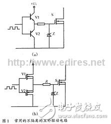
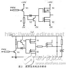
Switching power supplies have become more and more popular due to their small size, light weight and high efficiency. MOSFETs have become one of the most commonly used power switching devices for switching power supplies due to their fast switching speed, easy paralleling, and low required drive power. The quality of the drive circuit directly affects the reliability and performance of the switching power supply. The requirements for a good MOSFET driver circuit are: (1) The switching transistor is turned on instantaneously, and the driving circuit should be able to provide a sufficiently large charging current to rapidly increase the voltage between the gate and source of the MOSFET to the required value, to ensure that the switching transistor can be quickly turned on and there is no high frequency oscillation of the rising edge; (2) The driving circuit during the on-time of the switch tube can ensure that the voltage between the gate and source of the MOSFET remains stable and reliably conducts; (3) The turn-off instant drive circuit can provide a path with as low impedance as possible for the rapid discharge of the capacitor voltage between the gate and source of the MOSFET, ensuring that the switch can be quickly turned off; (4) The drive circuit during off period preferably provides a certain negative voltage to avoid mis-conduction caused by interference; (5) In addition, the drive circuit structure is required to be simple and reliable, and the loss is small, and it is preferable to have isolation. This paper introduces and discusses several simple and feasible MOSFET tube drive circuits used by the author in the development of switching power supplies. Introduction and analysis of several MOSFET drive circuits Non-isolated complementary drive circuit Figure 1 (a) is a commonly used low-power drive circuit, which is simple, reliable and low in cost. Suitable for small power switching devices that do not require isolation. The driving circuit shown in Figure 1(b) has a fast switching speed and strong driving capability. In order to prevent the two MOSFETs from being through, a small 0.5~1Ω resistor is usually connected in series for current limiting. The circuit is suitable for medium power that does not require isolation. Switching device. These two circuit structures are extremely simple. The power MOSFET is a voltage type control device that is turned on as long as the voltage applied between the gate and the source exceeds its threshold voltage. Due to the junction capacitance of the MOSFET, a sudden rise in voltage across the drain and source when turned off will cause an interference voltage across the gate and source through the junction capacitance. The commonly used complementary drive circuit has a small off-circuit impedance and a fast turn-off speed, but it cannot provide a negative voltage, so its anti-interference is poor. In order to improve the anti-interference of the circuit, a circuit composed of V1, V2, and R can be added to the driving circuit to generate a negative voltage. The circuit schematic is shown in Fig. 2(a). When V1 is turned on, V2 is turned off, the gate and source of the upper tube of the two MOSFETs are discharged, and the gate and source of the lower tube are charged, that is, the upper tube is turned off, and the lower tube is turned on, then the driven power tube is driven. When V1 is turned off, V2 is turned on, the upper tube is turned on, and the lower tube is turned off, so that the driven tube is turned on. Because the gate and source of the upper and lower tubes are discarded and discharged through different circuits, the loop containing V2 will continue to be saturated and turned off due to V2, so the conduction is slower than S1 for S1. The conduction is faster than the shutdown, so the degree of heat generation of the two tubes is not exactly the same, and S1 is more severe than S2. The disadvantage of this driving circuit is that it requires dual power supply, and since the value of R cannot be too large, V1 will be deeply saturated and affect the shutdown speed, so there will be a certain loss on R. Another circuit similar to that shown in Figure 2(b) is that it requires only a single power supply. The resulting negative voltage is provided by a 5.2V Zener. At the same time, the PNP tube is replaced with an NPN tube. In the two MOSFETs in the circuit, the heat generation of the upper tube is lighter than that of the lower tube, and the working principle is the same as the driving circuit analyzed above, so it will not be described again. --------------------------- More power technology hot text can pay attention to the latest "Power Technology Special Issue" 3 Phase Panel Voltage Meter,3 Phase Meter Panel,Panel Voltage Meter,Analog Panel Voltmeter TRANCHART Electrical and Machinery Co.,LTD , https://www.tranchart-electrical.com

