0 Preface This article refers to the address: http:// DELL chromebook 11 3110, dell chromebook 3110, ddell chromebook 3110 2-in-1 S-yuan Electronic Technology Limited , https://www.laptoppalmrest.com
Voice communication is one of the most commonly used communication methods in digital communication systems. An excellent speech codec algorithm can save bandwidth resources more effectively and improve frequency utilization. Nowadays, speech coding technology can be widely used in many military fields such as voice multiplex transmission, satellite communication, and secure communication. AMBE-2000, introduced by Digital Voice System Inc., is a high-performance, low-power real-time codec chip based on advanced multi-band excitation speech coding algorithm. It is adjustable from 2 000 to 9 600 b/s and has many functions such as forward error correction (FEC), voice activation detection (VAD), and dual tone multi-frequency (DTMF) signal detection.
1 Introduction to the system The main function of this speech system is to realize the mutual conversion of digital voice and analog voice and process the encoding and decoding of voice data, reduce the transmission rate of voice data, improve the frequency resource utilization of the system, and meet the interface requirements of the information system. . The analog voice portion is connected to the earphone microphone group, the digital portion compressed data stream is connected to the external processor, and the decompressed data stream is used for long-distance transmission of voice quantization information. The block diagram of the entire speech system is shown in Figure 1. 
When the voice is sent, the voice processing board performs A/D sampling quantization on the analog voice, and then is compressed and packaged by the voice codec chip and sent to the information processor for subsequent processing through the CPCI bus or the LVDS serial bus; or through the high speed RS 422 The serial port converts the voice quantized information transmitted from a long distance to the information processor for subsequent processing through the CPCI bus or the LVDS serial bus.
When receiving voice, the compressed data is received through the CPCI bus or the LVDS serial bus, and the voice is converted into an analog signal by D/A conversion after being decoded by the voice codec chip; or the received compressed data is decompressed and passed through the high speed RS 422. The serial port is transmitted remotely.
2 AMBE-2000 Features and Features The AMBE-2000 chip is an improved AMBE-1000 product. Compared with AMBE-1000, its speech compression algorithm is more optimized, the speech quality is higher, and the minimum coding rate is reduced from 2 400 b/s to 2 000 b/s. In terms of hardware and interface, several improvements have been made and the efficiency and reliability of compression coding and forward error correction coding (FEC) have been improved. The internal calculation is small and the power consumption is low. Its algorithm complexity is 13 MIPS (million instructions per second), which can achieve lower power consumption: only 65 mW at 3.3 V and only O at deep sleep. 11 mW.
In the simple model, AMBE-2000 is seen as two separate originals, encoders and decoders. The encoder receives speech quantization information (16-bit linear, 8-bit A-law or 8-bit μ-law) and outputs the compressed data stream to the channel at a desired rate. Conversely, the decoder receives the channel compressed data stream and synthesizes the voice quantized information. The time control of the AMBE-2000 encoder/decoder interface is completely asynchronous. Usually the voice interface is connected to the A/D and D/A chips. The input and output voice data streams must be the same. Format (16-bit linear, 8-bit A-law, or 8-bit μ-law). The system uses AMBE-2000 and the A/DD/A chip uses 16-bit linear sampling AD73311 to maintain compatibility with a previously designed AMBE-1000 based voice system. Based on the AMBE-1000 old-style voice system, the oversized, high-power 16-bit linear A/D and D/A chip TI32044 is used, and a series of peripheral chips with the same disadvantages are adopted, which is not suitable for low power consumption. , the development trend of small size.
3 AMBE-2000 interface design with A/DD/A chip The voice data stream format between A/DD/A chip and AMBE-2000 should be matched, that is, there must be a unified format (16-bit linear, 8- Bit A law, or 8-bμ law), in general, it is recommended to use 16-bit linear components. In this design, the AD73311 of AD Company was selected. The AMBE-2000 voice interface can be set to communicate specifically with the AD73311 by configuring hardware pins 84, 85 (CODEC_SEL[1-0]=01b). Therefore, the combination of AMBE-2000 and AD73311 will make the circuit design simpler.
Main features of AD73311:
(1) Low-power 16-bit A/DD/A converter with input/output sampling rate and gain can be controlled by software to provide a signal-to-noise ratio of 70 dB over the band. It is simple and efficient to transmit voice data through the serial port and receive control commands.
(2) The input analog audio signal passes through the variable gain amplifier, and the A/D converter converts it into a digital signal and outputs it through the serial port; otherwise, the digital stream from the serial port is converted into an analog signal and then output through a variable gain amplifier.
(3) There are two main working modes of AD73311: programming mode and data mode. After the chip is reset, it is in the default programming mode. At this time, the control word can be written to the control register through the serial port to set the working state. It should be noted here that the AD73311 should be placed in the corresponding format in the 3 V low power state (as shown in Figure 2). 
(4) After power-on reset, the AMEC-2000's CODEC_TX_DATA signal should be isolated from the serial input of the AD73311 and kept at about 365 ms. At this time, configure the AD73311 with the FPGA. The configuration words are as follows: 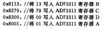
After setting, register A is written to Q1, indicating that it enters “data modeâ€. The CODEC_TX_DATA signal of AMBE-2000 should be connected to the serial input of AD73311, which can perform normal data transmission.
4 AMBE-2000 interface design with channel AMBE-2000 requires that the encoder be read by the controller once every 20 ms. After the reset, the initial frame is ready, the EPR changes from high to low, and then one frame of data is prepared every 20 ms. Accordingly, the external controller also needs to read one data frame every 20 ms.
The EPR pulse appears once every 20 ms, which is also an important basis for judging whether AMBE-2000 is working properly. The entire process of reading data is:
(1) Waiting for less than 20 ms;
(2) transmitting a frame synchronization signal, reading AMBE-2000 one frame serial output data;
(3) If the received data is not 0x13EC, it means that it is not the data frame header, discard the frame and re-execute the step, (2).
(4) If the data of the receiving port is 0x13EC, the remaining 23 words of the packet are read.
In this design, an FPGA is used as an external controller. The FPGA generates input/output frame sync signals, input/output clock signals, and serial input data of the AMBE-2000, and exchanges data with the AMBE-2000 in accordance with the timing relationship required by AMBE-2000. 
Table 1 lists the characteristics of the channel interface signal of AMBE-2000. The data transmission mode with the external controller is shown in Figure 3 and Figure 4.
5 system peripheral interface design The system's peripheral interface includes: CPCI interface circuit; conversion circuit between LVTTL and standard LVDS level signal; conversion circuit between LVTTL and standard RS 422 level signal; analog circuit.
5.1 CPCI interface circuit The CPCI-dedicated bridge chip can avoid complex PCI protocols and rapidly develop products. Therefore, PLX's high-performance dedicated bridge chip PCI9054 is used to implement the CPCI interface design. The CPCI interface design is completed by using the internal IP core of the FPGA to generate dual ports and establishing the glue logic with the CPCI part.
5.2 LVTTL and standard LVDS level conversion circuit In this system, in addition to the standard CPCI bus form to achieve digital partial compression data stream and external communication equipment data exchange, but also spare LVDS serial bus mode transmission, requires transmission The rate can reach 100 Mb/s. The system uses the MAX9129 and MAX9122 bus low-voltage differential signal drivers as drivers for LVTTL and standard LVDS level signal conversion circuits.
5.3 Conversion circuit between LVTTL and standard RS 422 level The decompressed voice data stream and the external digital audio equipment data exchange are transmitted in the standard RS 422 serial bus mode, requiring a transmission rate of up to 5 Mb/s. This system uses the MAX3491 low-power RS ​​485/RS 422 transceiver as a driver for LVTTL and standard RS 422 level signal conversion circuits for data transmission over long distances. The MAX3491 includes one driver and one receiver per chip for a maximum transfer rate of 10 Mb/s.
5.4 Analog Circuit The analog amplifier circuit consists of an op amp and some group of container parts. The main function is to use a high-performance, low-noise amplifier to adjust the gain of the input/output speech signal through a potentiometer or an appropriate proportional resistor.
The designed audio interface circuit adopts active balanced input/output voice transmission mode, which plays the role of differential mode amplification and common mode suppression, and improves the anti-interference ability. In the early days of audio production, transformers were often used to correct ground potential differences between different devices and to eliminate electrical noise generated in the cable lines. It also connects active devices with unbalanced high-impedance characteristics inside and balanced transmission lines with lower impedance characteristics. But transformers increase costs, increase system weight, and transformers sometimes introduce system distortion. Therefore, designers are constantly looking for ways to remove the transformer, and as a result, an active balanced input/output circuit is found.
6 Conclusion The voice system structure adopts 6U CPCI standard board, half-duplex working mode, within the voice bandwidth of 300-3400Hz, the intelligibility of tested speech words is greater than or equal to 90%, the intelligibility of speech sentences reaches 100%, intonation. Natural, clear pronunciation, is a high quality voice system.