Abstract: Based on the ICX229AK CCD chipset, an integrated camera with VGA interface is designed. The DSP+FPGA+ASIC architecture is used to complete the acquisition of video signals and multi-format display. Auto focus, auto iris and other functions are realized in the FPGA, and the practical functions such as mouse driving, scribing, and OSD display are expanded. Through PWl226 filter amplification processing, the conversion of PAL digital video signal to VGA format is completed, and the resolution can reach 1 024x768. Simultaneous output of composite video, S-VIDEO and VGA video signals is realized. The integrated camera can be used for video booths and real-time monitoring, which greatly improves the output image quality. This article refers to the address: http:// We are manufacturer/supplier of USB flash drive from China,who offer 100% real original capacity to the world buyers.You can get high quality of USB flash drive from us with custom logo,and also help you build your own brand of USB flash drive 2.0 3.0 with reputation.Capacity from 2MB,8MB,64MB,128MB to 8GB 16GB 32GB 64GB 128GB and 256GB(Biggest real capacity can be 512GB).We mainly offer OEM /ODM service,and offer USB flash drive without logo or with your logos. Usb Flash Memory,Usb Flash Drive 32Gb,Usb Flash Drive Custom,Usb Flash Drive 3.0,USB Disk,Pendrive,USB key Shenzhen Konchang Electronic Technology Co.,Ltd , https://www.konchang.com
Keywords: PAL; VGA; FPGA; auto focus; image magnification
The integrated camera is widely used in monitoring, education, medicine and other fields due to its compact size, low price and easy installation. The integrated camera is designed according to the conditions and requirements of the object to be used. Based on the parallel processing capability of FPGA devices and the flexibility of reprogrammability, a system solution based on DSP+FPGA+ASIC is proposed, which improves the difficulty of expanding the function of integrated cameras in the past and improves the image. Quality has expanded its range of applications.
1 system hardware design System hardware block diagram shown in Figure l. The video acquisition module uses SONY's camera kit, which mainly includes 470 K pixel PAL CCDICX229AK, AFE (analog front end) CXA2096N and dedicated DSPCXD4103. The module firstly processes the image data collected by the CCD and outputs the digital video signal of the PAL YUV (422) ITUREC656 format with a resolution of 748x584, and simultaneously outputs the line, field reference signal and pixel clock signal. These signals are first passed through the FPGA image processing module to achieve auto focus, 4 image storage, mouse drive and scribing functions, real-time image and storage image up and down, left and right contrast, OSD overlay, image freeze, negative display, mirror, color black and white selection output, etc. Features. The processed signal is finally sent to the video display module, and processed by the dedicated integrated circuit (PWl226) to generate RGB image signals and standard SVGA format line and field sync signals, so that the images captured by the image sensor can be displayed in real time on the VGA display. 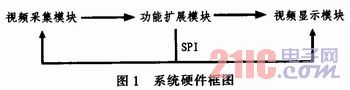
1.1 Video Capture Module Figure 2 shows the hardware block diagram of the video capture module. After the system is powered on, the DSP reads the initialization information from the EEPROM. After the initialization is completed, the DSP generates a CCD line and field timing signal, and simultaneously generates a sampling timing signal of the AFE (Analog Front End). The CCD sends the collected raw image data under the action of line and field timing. After the AFE undergoes CDS (correlated double sampling) and AGC (automatic gain control), the quantized signal is sent to the DSP. The DSP's built-in 10-bit ADC converts the quantized signal into a digital signal, and performs noise filtering, level clamping, auto white balance, edge enhancement, etc., and outputs digital video in PAL YUV (4:2:2) format. signal. At the same time, the DSP directly outputs composite video and S-VIDEO. 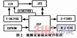
The CCD peripheral circuit design is shown in Figure 3. The ICX229AK is a 1/4-inch PAL complementary image sensor with an effective resolution of 752 (H) x 582 (V) for PAL, 12 V operating voltage, 14-pin DIP package, and high sensitivity with ultra-HAD technology. And can obtain high-saturation video signals; has the advantages of fine picture quality, bright colors, high signal-to-noise ratio. 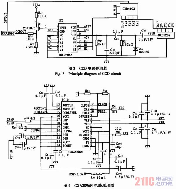
The CCD is powered by a 12 V and -5 V power supply. The DSP timing generator simultaneously outputs the line and field timing drive signals. The field drive signals are amplified and integrated by CXDl267 to generate field timing drive signals V1, V2, V3, and V4 for the CCD. The line signals H1 and H2 sent by the DSP are simultaneously sent to the CCD to start normal operation, and the collected electric signal is amplified by the FET 2SKl875 to obtain an analog output signal CCDOUT, which is sent to the sampling circuit CXA2096.
C27, R27, VD6, C23 form a bootstrap boost circuit, which converts the VSUB signal from CXDl267 into a voltage amplitude acceptable to the CCD, that is, the SUB signal, which is an electronic shutter control signal that controls the charge accumulation time on the sensor pixel surface. Operate the shutter. When the electronic shutter is closed, the CCD charge accumulation time is 1/50 s for the PAL camera. The electronic shutter is covered by a basic unit of 311 steps, which ranges from 1/50 to 1/10 000 s. As the electronic shutter speed increases, the amount of light focused on the CCD decreases during the time allowed for each video field, with the result that the sensitivity of the camera is reduced.
AFE peripheral circuit design is shown in Figure 4.
The CXA2096N is powered by a 3.3 V. Its main function is to sample, hold, and amplify analog electrical signals. The package is a 24-pin SSOP (Plastic). The analog signal CCD-OUT sent by the CCD is amplified by 2SKl875 and transmitted to CXA2096N. After being sampled, held and amplified by CXA2096N, the DRVOUT signal is transmitted to the DSP. The CXA2096N is the last link before the analog-to-digital conversion of the signal. The importance is self-evident. Similarly, the CXA2096N also performs a series of operations under the timing drive signal of the DSP clock generator. The three most important signals are CCDLEVEL, OFFSET, and AGCCONT.
CCDLEVEL is the output signal of CXA2096N. This signal directly reflects the level, degree and extent of the signal collected by the CCD. The black level signal collected by the CCD under normal conditions is about 2.7 V.
OFFSET is the output signal of CXA2096N, the range of variation is 1.5~3 V. This signal reflects an offset. The DSP can change the sampling bias voltage of CXA2096N. This change is directly reflected in the video display processing board. Reflected in the final image display. The larger the OFFSET, the larger the image changes to a brighter area, and vice versa. Because the OFFSET signal causes the overall offset of the image to change, using an image metaphor, it is an "plus" relationship, that is, the image data is increased by a bias level as a whole. AGCCONT is also the output signal of CXA2096N, the range of variation is 1.5~3 V. This signal reflects a gain amount. All integrated cameras have a signal from CCD amplified to a levelable video amplifier. The amplification is gain, etc. It is sensitive to higher sensitivity and makes it sensitive to low light. However, in bright lighting environment, the amplifier will be overloaded and the video signal will be distorted. To this end, it is necessary to use the automatic gain control (AGC) circuit of the integrated camera to detect the level of the video signal, and switch the AGC in time, so that the camera can work in a large illumination range, that is, the dynamic range, in low illumination. Automatically increase the sensitivity of the camera to increase the intensity of the image signal for a clear image. The external MCU or DSP can directly reflect the amplification gain coefficient of the CXA2096N in the video display processing board to reflect the final image display effect. The larger the AGCCONT, the larger the image changes to a brighter area, and vice versa. Because the AGCCONT signal causes the overall offset of the image to change, that is, the image data as a whole "multiplies" the gain factor.
The sampling of CXA2096N requires a reference voltage, otherwise the sampled data will be biased, which has a great impact on future video data processing. The sampling calibration voltages VRT and VRB must be accurate. The VRT is 2.35 V, which is the upper sampling limit: VRB is 1.35 V, which is the lower sampling limit. At the same time, VRT and VRB are output to the A/D converter as their quantized reference level.
1.2 FPGA Image Processing Module The logical structure of this module is shown in Figure 5. The module is based on an FPGA design that implements autofocus, auto iris control, frame rate boost, OSD, and SPI communication. The FPGA uses the XC3S250E from XILI-NX. The internal function adopts a top-down hierarchical design method and is implemented in VHDL hardware description language. Finally, ISE 6.0 comprehensively generates a bit stream and solidifies it in external memory. 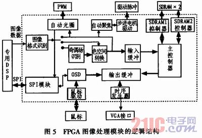
The FPGA recognizes and converts the received YUV (4:2:2) format signal, and then buffers two consecutive fields of image into one frame image in SDRAM, and the next frame image is buffered in another SDRAM to form a continuous image. Switch the video double buffer structure. When one of the SDRAMs inputs an image, the other slice outputs an image at a point rate of SVGA@60Hz through the output FIFO under the control of the VGA display controller. The specific process is as follows:
The module first performs parity field identification on the input signal. The first line of the odd field scan has 374 pixels, and the first line of the even field scan has 748 pixels. The first field of the field is counted and judged, and the current field is known. It is an odd field or an even field, and then receives data from the next odd field. This ensures that the adjacent two fields are a complete image of one frame. This module is a deep 748, 16-bit asynchronous FIFO (first in, first out), writes a loop counter with an address counter of 0 to 748. When it counts to 300 or 700, it sends a read signal to the main controller, and the main controller then The FIFO read enable signal is generated so that the read enable signal is asserted for 374 consecutive read clock cycles, and 374 data can be read continuously. The design read clock frequency is greater than the write clock frequency, and there is no data overflow and overflow.
The main controller realizes the switching of the read and write operations of the two SDRAMs by processing the read request signal of the input buffer and the write request signal of the output buffer. The module first completes the initialization of the SDRAM, and the SDRAM is set to a continuous full page advance mode. Then the SDRAM enters the normal working state and is ready to receive read and write commands. When the SDRAM is in the idle state, in order to keep its data from being lost, it must be refreshed periodically. Generally, it needs to be refreshed 4096 times within 64ms. However, when the SDRAM is reading and writing, the auto-refresh command will interrupt reading and writing. This causes data loss. The design performs at least 4,096 read and write operations on the SDRAM in 64 ms, so it is not necessary to refresh it. When the SDRAM reads and writes to 374, it issues a precharge command to stop the advance, and closes the current line, ready for the next read and write. The SDRAM is set to the incoming mode with a length of 374.
First, the timing generator uses the 40 MHz master clock to generate the line and field sync signals conforming to the VESA standard, while the line and field reference signals are valid, and the output buffer is generated when the 39<row counter <788, 19<field counter <604. Read enable signal. The output module is an asynchronous FIFO with a depth of 748 and a width of 16 bits. The write clock and the read clock are both 40 MHz master clocks. When the read enable is active, the read counter is started counting from 0 to 799 cycles. The design reads the previous data repeatedly every 10 data until 800 data is output. When the read counter counts to 100 or 500, the module issues a request command to the main controller module. During line and field blanking, the read enable signal is invalid, so no read error occurs.
The PWl226 video display module further filters, eliminates the flicker effect between the lines, improves the picture quality, and smoothly scales up to the resolution of l 024x768, and finally outputs the standard VGA video interface signal of SVGA or XGA.
At the same time, the FPGA can also set the registers of DSP and CXD4103 through the internal SPI module to make it work normally.
1.3 Auto Focus First, the FPGA implements the auto focus function by processing the image brightness signal Y. The commonly used gray-scale difference method is selected as the focus evaluation function, and the difference values ​​are calculated by selecting the past four pixels of the center pixel (the left side, the upper left side, the right side, and the upper right side of the four pixels).
Since the focus evaluation function needs to use the center pixel and the adjacent row of 4 pixels, it is necessary to use two dual-port RAMs in the FPGA to make two adjacent rows of data buffers, each of which has a capacity of 800x8 bits. The read/write selection module writes the first line of data of one frame of image to RAM1 and the second line of data to RAM2. After writing to RAM2 for one clock cycle, the data in RAM1 and RAM2 are read out, and sent to the focus evaluation function algorithm implementation module to calculate the absolute value of the luminance difference value as the center pixel of the image pixel in RAM2, and when the image is in the third line When the data arrives, it is written to RAM1 again. After writing to RAM1 for one clock cycle, the data in RAM1 and RAM2 are read out and sent to the focus evaluation function algorithm implementation module. The absolute value of the luminance difference is also calculated centering on the pixel in RAM1. And, in this loop, get the sum of the absolute values ​​of the luminance differences of one field.
Figure 6 is a focus evaluation function implementation module. In the figure, the focus evaluation function realizes two rows of data read by the module, and the row of the central pixel is selected by writing to the register selection module, and the second column register is written. Under the clock synchronization, each clock shifts the pixel right to the next register, and the data in the registers regll, regl2, regl3, reg2l and the data in reg22 are subtracted, and the differences suml, sum2, sum3, sum4 are added. Get and sum. When a frame of image ends, the data in sum becomes the sum of the luminance differences of the frame. The result of the current frame calculation is compared with the calculation result of the previous frame. If the function value of the current frame is larger than the function value of the previous frame, indicating that the current image is clearer than the previous frame image, the output result OUT is '1', and vice versa. Output '0'. 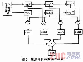
The hill-climbing search algorithm is used to determine the optical focus position. After the auto focus enable signal is valid, the drive motor rotates 8 steps from the initial position, reverses 8 steps, then reverses 8 steps, and forwards 8 steps to return to the initial position. The output out value of the focus evaluation function module is detected in 1 step, and the number of '1' detected in 4 8 steps is saved as suml, sum2, sum3 sum4, and then statistical analysis is performed. If suml≥16, then It is considered that the forward direction is the focus direction; if sum2≥6, the reverse direction is considered to be the focus direction; if both suml and sum2 are not greater than or equal to 6, the suml+sum4 and sum2+sum3 are calculated; if suml+sum4≥sum2+sum3, Then, the forward direction is considered to be the focus direction, otherwise the reverse direction is considered to be the focus direction. After determining the focus direction, the stepping motor is driven to drive the lens to rotate step by step in the focus direction. The output OUT value of the focus evaluation function algorithm module is detected in one step. If the 2-step output out of the continuous rotation is '0', it is considered to be the most The clear position drives the stepper motor back 2 steps and the lens reaches the best focus position.
The stepper motor drive includes a zoom motor drive and a focus motor drive, the zoom motor achieves zooming, and the focus motor is used for focusing. The zoom motor and the focus motor are excited in different ways. The zoom motor uses a 2-phase excitation method, as shown in Table 1. The focus motor uses the 1.2 phase excitation method, see Table 2. Among them, A+ and A- respectively represent the positive-end and negative-end power bridge control signals of the A-phase winding, and B+ and B- respectively represent the positive-end and negative-end power bridge control signals of the B-phase winding. According to the level signal shown in the table, it is applied to the two sets of coils of the stepping motor, and the torque generated by the phase difference between the coils is used to drive the motor stepping work. According to the pulse sequence shown in the table, the stepping motor can be reversed by changing from left to right; otherwise, forward rotation is achieved. Taking the zoom motor drive as an example, a state machine is designed in the FP-GA to realize state transition between four states. When each zoom enable is enabled, according to the current state transition, the zoom direction shifts to the next adjacent state. The four control level signals corresponding to the state are output, and the driving motor is rotated to realize the zoom function. It should be noted that since the driving level and current of the FPGA output pulse signal do not match the driving requirements of the stepping motor, the driver bridge circuit should be connected to the FPGA output pin. 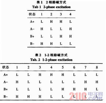
1.4 Auto iris control The brightness of the image is related to ambient light and aperture. The auto iris control determines the target aperture aperture by calculating the brightness of the image at a specific illumination level, thereby obtaining an image with appropriate exposure. Through experiments, the relationship between illuminance (corresponding to image brightness) and HALL voltage value (δ1 ~ δ5) is given, as shown in Fig. 7. By changing the aperture aperture and calculating the corresponding image brightness value to obtain the coordinates of 2 points on the curve, the curve corresponding to the current illuminance can be determined. The intersection of the curve and the line corresponding to the reference luminosity value is the target HALL voltage value (target aperture aperture). 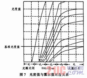
Since the curve is non-linear, the curve is stored in the FPGA by creating a lookup table. The horizontal axis is divided into δ1 to δ55 regions, and each region can be approximated by a straight line, and the slope of the straight line and the starting point coordinates are stored in the lookup table. The current control curve can be determined by the aperture aperture value (corresponding to the circuit HALL voltage value) and the corresponding luminosity value. If the aperture aperture value is at the boundary point, the aperture motor should move to the inside of the area so that the 2 points are all in the same area, ensuring that the 2 points are on a straight line.
By determining the luminosity curve, you can adjust the aperture opening along the curve. The intersection of the reference illuminance horizontal line and the determined luminosity curve necessarily corresponds to a specific aperture opening value (a specific HALL voltage value). In the specific operation, it is only necessary to drive the aperture motor to change the aperture aperture until the CPU obtains the specified HALL voltage value, which is the optimal exposure state.
1.5 OSD (On Sereen Display) Module The most important aspect of OSD design is the video mouse, which is based on the mouse display in SVGA format. The module first uses a 40 MHz master clock to generate line and field sync signals in a standard SVGA format with a resolution of 800x600 and a frame rate of 60Hz in accordance with the VESA (Video Electronics Standardization Association) standard, while the line and field reference signals are valid. Generates an enable signal to the output buffer module as a read enable for the output buffer. When the line counter is equal to the coordinates of the mouse on the screen, the mouse is displayed, otherwise the image output after interpolation is displayed.
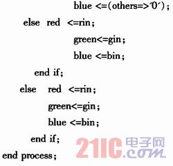
For example, if the mouse is displayed as a red rectangle, its length is 30 pixels, the width is 10 pixels, and the upper left is the coordinate determined by the displacement of the mouse in the horizontal and vertical directions. The VHDL described in this section is described as: 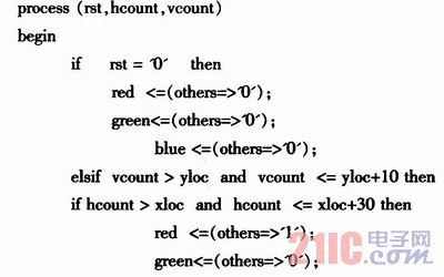
According to actual needs, the mouse can also be displayed in other colors and shapes, and is suitable for display formats such as XGA.
2 Conclusion Based on FPGA, an integrated camera with multiple output interfaces is designed. Real-time display of high-resolution images is realized by FPGA, which adds auto focus, auto iris control, image freeze, negative display, graphic text selection, color black and white selection. OSD display and other functions. And the FPGA still has a lot of ports for function expansion. The system design integrates various image processing algorithms and system control functions into a single FPGA, so that the video output has three output interface forms at the same time, which expands the application range of the all-in-one. The system has good upgradeability in both hardware architecture and FPGA internal logic function implementation. In the PCB design process, attention should be paid to the integrity problem of high-speed digital signals and the noise interference of analog-digital hybrid design to avoid the adverse effects caused by hardware design.
In further research, functions such as image flipping can also be realized, and the image enlargement algorithm can be improved to obtain better image quality. The design can be applied to real-time monitoring, digital video booths, etc., with the advantages of high real-time performance, good image quality, and expandable functions.