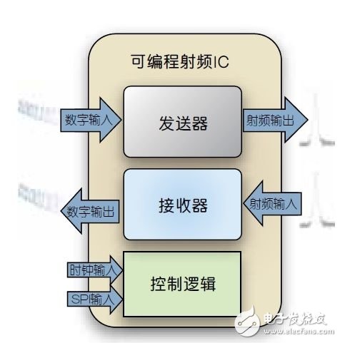
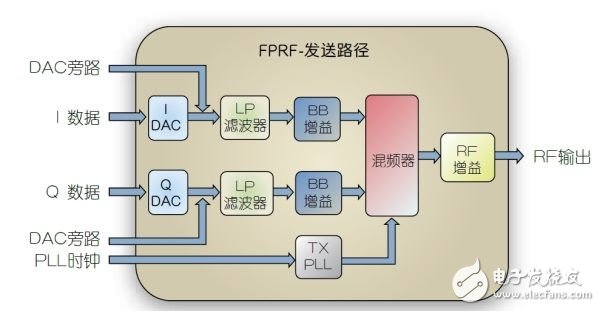
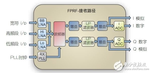
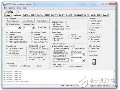
As we all know, FPGAs have evolved from simple glue logic integration to the ability to implement complex digital functions. In this process, FPGAs include a wide variety of hard-logic cores and functions, such as processors and dedicated interface modules. Some FPGAs also have sophisticated analog functions such as high-speed transceivers, but in general, FPGAs actually reach the edge of the analog world. In contrast, field-programmable radio frequency chips (FPRFs) originated in the wireless field, which have given people exciting new possibilities. At the highest level of abstraction, the FPRF transmitter accepts digitized data streams and converts them into wireless signals. At the same time the receiver performs the opposite operation. There are also functions for programming key parameters such as RF frequency, gain, and bandwidth. Usually a FPRF chip contains several major parts shown in block 1: Figure 1: Several major components of the FPRF chip When I first learned about this device, I discovered that the RF functionality it brings is somewhat similar to what FPGAs offer in the logical domain. First, it is programmed by the customer rather than programmed in the factory. Second, supporting tools allow customers to conduct online tests and modify parameters. The third and most important point is that the scope of application is limited only by the user's imagination. This FPRF chip was manufactured in the United States by a British company called Lime Microsystems. The part number is LMS6002D, but Lime created the new acronym FPRF because it captures the essence of the product. Let's take a closer look at this product. Wireless transmission uses a variety of different modulation schemes while the chip accepts data in the form of in-phase (I data) and quadrature (Q data) words. In the transmit path, data is first converted into two analog signals by a pair of on-chip digital-to-analog converters (DACs). The user can choose to bypass these DACs and inject the analog signal directly into the device or monitor the DAC output. The next step is to filter the signal. The passband of this filter is programmed by the user to one of 16 different bandwidths ranging from 1.5 MHz to 28 MHz. Filtering limits the signal to the selected bandwidth and attenuates any out-of-band noise or aliased signals from the DAC. The following is a block diagram of the transmit (TX) path: Figure 2: Block Diagram of the Transmit (TX) Path The filter can boost the signal by 6dB, followed by a programmable baseband gain circuit that can be adjusted to provide up to 31dB gain in 1dB increments. The signal is then mixed directly to provide the desired modulated RF output. The transmit PLL synthesizer multiplies the input PLL clock by a programmable ratio and then produces a stable frequency with tight precision. The RF gain stage circuit (of course, programmable) provides the final signal boost from the FPRF device output. Sending power levels without any further amplification is enough for short-range communications, such as tens of meters. Users can use an external amplifier circuit to increase the communication distance. Not surprisingly, the receive path is also highly programmable. The FPRF device offers three low noise amplifier (LNA) options. The universal wideband input circuit is designed to handle RF input signals in the frequency spectrum from 300MHz to 3.8GHz. To enhance performance, the other two low-noise amplifiers are optimized for 300 MHz to 2.8 GHz (Lo LNA) and 1.5 GHz to 3.8 GHz (Hi LNA) signals, respectively. The following gives: Figure 1: Several major components of the FPRF chip The mixers in the receive path use the same PLL clock input as the transmitter, but use different synthesizers to provide full-duplex and direct down conversion. Before the analog signals are digitized and output as I&Q data streams, programmable gain and filter circuits are also required. All the different unit configurations are programmed into the control logic through a simple SPI interface. Each cell is programmed by loading a 16-bit word. This process can be static. For more complex applications, parameters can also be changed online. The configuration is done using a simple graphical user interface that controls the above functions as well as test and loop modes. The graphical user interface looks like this: Figure 4: Graphical user interface for controlling FPRF devices At this point we have considered a brief description of the technical details of the device - but what can you do with it? Well, this chip is designed to be very flexible because one of its key applications is femtocells and picocells, which I explain in detail below. These boxes serve as local base stations for cell phones and are linked into the Internet to provide quick connections at home or in small offices. For example, the nearest base station in my house is on the other side of the mountain, so my receiving signal is very unstable. Femtocells allow me to no longer rely on signals from base stations. The challenge for designing RF chips for these applications is that the cellular systems around the world are different, and 4G or LTE handsets need to be truly global and may require more than 40 different combinations. So FPRF designers had to be made programmable to avoid being limited to a single market. Once your chip covers all cellular frequencies, you will cover many other applications. For example, changing television transmissions from analog to digital can release a bunch of spectrum for new wireless services. These spectrums are called “blank television signal bands†and many companies are working hard to develop a wide variety of products ranging from home appliances, smart meter reading, machine-to-machine (M2M) and rural broadband. The spectrum analyzer is an application Lime uses to demonstrate. The receiver in the chip scans and listens to all frequencies on the above frequency band, and the instantaneous output is displayed as a spectrogram. This application demonstrates the ability of the FPRF chip to change quickly and dynamically. The military system maker quickly seized this opportunity and is working on designing a Software Defined Radio (SDR) system. But only when you combine FPGAs and FPRFs does things really become interesting. All modern wireless systems lack a large number of digital processing functions for adjusting signals and recovering data from noise. The Myriad-RF evaluation board can interface with TerAsic's Altera DeO-Nano boards and FPGA Mezzanine Card (FMC) Xilinx boards, including the entire 7-series product from ArTIx, all programmable FPGAs from Kintex and Virtex, and all Zynq programmable SoCs. The Myriad-RF interface board required for the above applications can be ordered through Azio. Simultaneous access to programmable radios and editable logic opens up new opportunities. For example, I have studied the possibility of using FPRF devices in university teaching and research. It will open up a variety of colorful applications. Researchers are considering the use of this device for cellular applications so that specific algorithms can be implemented in the logical domain and the results can be viewed at the RF output. On the other hand, FPRF can receive weak signals. Researchers can use FPGA to test different error correction mechanisms. Other possibilities include the use of FPRF chips for resource management algorithms for evaluating ad hoc networks, ground penetrating radar, or vehicle-to-vehicle communications. FPRF allows professionals and amateurs to access flexible wireless transceivers that will be used in many new products in the coming years. Of course, if you want to send a wireless signal, don't forget to confirm the power level and frequency allowed by local regulations.
Ungrouped,High Quality Ungrouped,Ungrouped Details, CN Shenzhen Waweis Technology Co., Ltd. , https://www.laptopsasdapter.com


