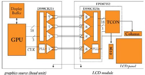
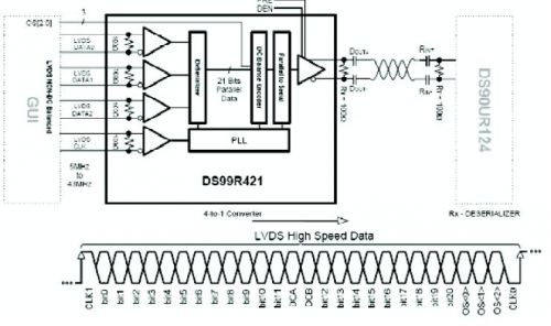
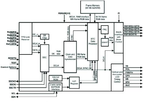
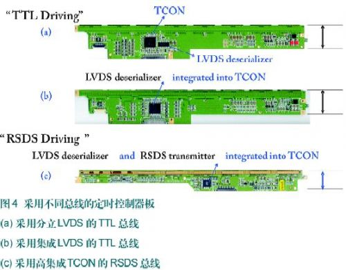
introduction This article refers to the address: http:// The large panel LCD market (LCD TV, desktop PC monitor, laptop monitor) is now moving toward high standardization and integration, and the automotive infotainment LCD architecture is in the traditional concept. The main reason is that the industry tends to buy a complete LCD module and concentrate on the video adapter or interface card design. Now, timing controllers (TCON) with basic TFT glass and displays with differentiated designs are becoming a new trend. In addition to the external LCD interface, internal display interfaces can also be considered, such as the current industry standard RSDS (Strain Suppression Differential Signaling) bus technology. The benefits of integration of internal and external interfaces are just a few examples: fewer components are used, PCB space is saved, and EMC radiation and magnetization benefits are reduced. This type of benefit also applies to image master applications, which typically occur within a car audio body ECU (electronic control unit). Today's image processing units (GPUs) are increasingly deprecating wide CMOS/TTL outputs because they consume a large number of package pins. Currently, more and more image source components provide a first stage of serialization based on serial data channels for color bit applications with parallel clock channels. With reference to the regulations of the open industry standard "FPD-Link" physical layer, it is expected that the flexibility of connection selection will be further improved in the future. In this way, the serialization of the first stage can be sublimated by using a bridge chip to provide a second stage of series connection on a single pair of interconnects in order to produce a slim and connectable cable connection scheme. Automotive housing wiring—especially applications that need to be connected to rear-seat entertainment displays—is especially important. Traditional image connection to remote LCD panel In traditional automotive infotainment system designs, an image controller or image processing unit (GPU) transmits parallel RGB color bits with pixel clock and sync signal alignment. As shown in Figure 1. In remote LCD display connections, the parallel bus cannot sometimes span more than 20-30 cm due to problems with the cable being too thick, or power and EMC (electromagnetic compatibility). In response to this problem, in the mid-1990s, National Semiconductor developed a new series of serialization/deserialization (SerDes) FPD-Link (Planar Display-Link) chipsets with leading TFT panel suppliers. The transmitter accepts up to 18 bits of RGB information (6-bit color depth mode) and three control signals and clocks, which are then converted into three differential data pairs and one clock pair. A complement function is set on the panel. The FPD-Link receiver deserializes the data stream and provides the pixel data and control signals to the TCON (timing controller) on the panel, which then reformats and routes the signal to the row and column drivers of the LCD glass. . The bitmap and signal format of the FPD-Link physical layer has become the standard set by the SPWG (Standard Panel Working Group) and is the industry standard connectivity solution for notebook LCD monitors. The chipset adopts the LVDS (Low Voltage Differential Signaling) physical layer standard: ANSI/TIA/EIA-644A. LVDS is a high-speed, low-power interface that is not only used in today's embedded displays, but also in a wide variety of data communications and telex communications that require high-speed data transmission. Its advantages include high speed line rates, low power consumption, and low noise and durability. In addition, its ability to eliminate common mode noise is twice as strong as a true differential signal. In this way, high-resolution panels can be supported via smaller interfaces, simplifying the design of the interconnect while still supporting panel resolution at all levels. The FPD-Link concept can also be extended to the more comprehensive "OpenLDI" (LVDS Display Interface) specification. OpenLDI details the logical, electrical, and mechanical characteristics of the interface between the display source and the display device that carries the digital display data. For long-haul wire-over applications over 10 meters, an enhanced version of LVDS SerDes can be adopted. The enhancements included in the transmitter are optional pre-emphasis and a simple low-power DC balancing scheme to open the eye diagram at the end of the lengthy cable. In addition, the receiver provides a cable back skew function that allows the use of standard double lines. In its "LVDS Non-DC Balanced" mode, the OpenLDI physical layer is backward compatible and identical to the FPD-Link physical layer. LVDS bridging concept between four-lane and single-lane series/inverting converters More and more image processors, scalers, and even mid- to low-end FPGAs now incorporate the FPD-Link physical layer. The main advantage of integration is the ability to distribute large data streams across multiple restricted medium-speed data channels and reduce the design risk of using high-frequency phase-locked loops (PLLs) and clock data recovery (CDR) circuits in complex digital chips. On the other hand, on the wiring of the car casing, the cable produced by the four-lane (eight cables) differential interconnection is still relatively thick and flexible. Cables longer than 5 meters may create potential skew between data and clock channels due to cable construction and specifications. In the installation of automobiles, since manufacturers tend to use AC-coupled connections to provide isolation for the displacement ground potential on the transmit and receive ends, a more logical solution is a single-track conversion scheme that includes an embedded clocking scheme. For image sources with FPD-Link interfaces, National Semiconductor's DS99R421 can combine four non-DC balanced LVDS lanes (three LVDS data plus one LVDS clock) with three oversampled low speed control bits (OS) <2:0>) is converted into a single LVDS DC balanced serial data stream with embedded clock information, as shown in Figure 2. This serialization scheme simplifies the task of converting a 24-bit bus on a single differential pair by eliminating skew between the data and clock paths. By narrowing the interconnect, it helps to reduce the number of layers of the PCB, the cable width, and the size and pins of the connector, saving system cost. In addition, the device integrates a 100Ω termination resistor at the LVDS input. In addition to the above, the device also features a pre-emphasis signal condition on the LVDS output to enhance the signal when using a lossy cable for longer connections. The user can control this function with an external resistor and drive shielded double turns up to 10 meters with a data throughput of up to 1032 Mbits per second. Internal DC balanced encoding supports AC-coupled interconnects through series capacitors. The DS99R421 serial data stream bit map is compatible with the DS90UR124 single-channel LVDS anti-serializer component and includes a "@Speed ​​BIST" (built-in self-test) feature to verify link integrity. RSDS optimized internal panel TFT-LCD architecture Automotive display system suppliers are increasingly focusing on the development of timing controllers to highlight the uniqueness of their products. Therefore, even internal display buses between TCON and row/column drivers are of interest. National Semiconductor has teamed up with leading LCD module suppliers to develop an open suppression swing differential signaling standard. The goal is to establish a common standard for the interface between the LCD timing controller and the column driver components. This interface, while supporting high data throughput, reduces the number and power consumption of interconnects and reduces electromagnetic emissions to simplify shielding. RSDS is actually a derivative of the industrial LVDS signal standard (RS-644A), and its output drive current is further reduced to only 2mA. The differential signal amplitude in a typical 100Ω termination resistor is only ±200mV, but this is sufficient for internal connections for short to medium distances. The edge rate swing due to relatively small signals during signal conversion can be designed to be moderately ramped, which results in a higher pixel clock frequency than the TTL signal. The RSDS output buffer provides a bias voltage of 1.3V as a common mode voltage for differential signaling. The RSDS bus only needs to propagate RGB color bits and a parallel clock signal ("RSCK"). RSDS uses a 2:1 multiplex scheme, which has a color bit on each data channel, and each bit is simultaneously multiplexed during the rising and falling edges of the clock channel ("double data rate") ). The receive column driver component can therefore operate without the need for an integrated high frequency PLL circuit, which facilitates its integration into or onto the glass substrate. Compared to the TTL bus concept, half of the bus lines can be reduced by this serialization. For example, in a TTL dual bus ("double and single pixel") architecture with 6-bit color depth, there are 36 data lines and two clock lines (38 lines in total), and in an equivalent RSDS architecture. There is only one bus at this point, which contains 9 data differential pairs and one differential clock pair (20 lines in total). Timing controller with integrated LVDS and RSDS interfaces The timing controller is the brain and core components of the TFT LCD module. For automotive remote displays, the input signal is in many cases provided by the serial LVDS data stream of the image master (eg, car audio body ECU). The LVDS interface functions in the inverse serializer function: it maps the RGB color bits and control signals (Hsync, Vsync and DE) back to a parallel data format. Next, TCON routes and reformats the data toward the row and column drivers of the LCE panel. For example, the FPD87532 shown in Figure 3 is an example of a highly integrated timing controller. The TCON in the figure combines an LVDS single pixel input interface with an RSDS output column driver interface and is placed next to the flat display to provide data buffering and control signal generation. The FPD-Link receiver with LVDS features four data channels and one clock channel to provide 24-bit color. In addition, the SSC (spread spectrum clocking) function reduces electromagnetic interference by distributing the axial peak energy over a wide frequency band. This feature uses an external SSC source that is responsible for providing synchronized spread spectrum to the RSDS and control signal outputs. The two-wire serial EEPROM interface controls the initialization of the LUT (Search List) register. If there is no EEPROM, the LUT data is provided by the internal ROM. The CLK and Data Synchronizer functions delay and align data to accommodate internal data processing including RSDS skew control. All data processing needs to be aligned by RSDS output and LCD timing control signal, and its RTC (Response Time Compensation) function can improve the internal gray level response time of the LCD panel to achieve better moving image display. The function of the RTC is achieved by applying a boost or overdrive voltage, which forces the liquid crystal material to react faster. This is especially important for automotive displays that operate at low temperatures because liquid crystal materials typically have a slower reaction rate at low temperatures. The boost pulse is controlled via an internal or external EEPROM LUT (which includes the boost/overdrive stage) plus external memory that can be used as a picture buffer. The reference value of the RTC is a new grayscale value whose value depends on the difference between the current frame RGB grayscale data of the same pixel and the previous frame RGB data. The RSDS interface converts CMOS-level signals into RSDS signals for system clock (DCLK) and RGB color data. RSDS skew can be controlled in several steps to accommodate different delays in the corresponding column drivers. The vertical and horizontal LCD timing control blocks generate TTL/CMOS level signals for connecting the column and row drivers in the LCD system. All signals are synchronized to the RSDS data clock. To demonstrate the integration benefits of the TCON solution, Figure 4 shows the benchmarks for the different generations of timing boards. As can be seen from the comparison, the number of external components and the size of the PCB are significantly reduced. For example, a 10-inch wide-screen VGA LCD with 190 passive components requires a TTL bus between the TCON and the column drivers. However, by using the RSDS bus, the number of components has been drastically reduced to only 101, with a frame drop of 47%. In addition, the number of layers of the PCB has been reduced from six layers at the time of TTL to four layers at the time of using RSDS, which further reduces the cost. Finally, EMC benefits from the need to use a wide parallel TTL/CMOS bus outside of the timing controller. Conclusion Modern automotive infotainment display architectures are increasingly phasing out to replace the old parallel TTL/CMOS RGB bus with an integrated series solution to create the perfect system concept. The advantage of this solution is the reduction in pin count, number of interconnects, power consumption, radiated emissions, and external noise. The LVDS and RSDS physical layer standards have been validated, and the related technologies have matured, which not only simplifies the design work but also greatly reduces the design risk. In the future, the integration on and within the LCD glass substrate will continue to increase. Timing controllers with basic functions will be available in COG (on-glass). In this case, the RSDS bus can be used as an alternative to the input bus. Because the RSDS receiver does not require a high frequency PLL structure that is difficult to integrate on the glass to gate the input data. The overall system performance can be improved by taking advantage of the system segmentation on the complete data path from the image control master via the intermediate interface adapter or TCON board, the board base to the chip components on or within the TFT glass. EMC features can also reduce the system. Incremental Encoder,Linear Scale Encoder,Dual Concentric Rotary Encoder,Dc Servo Motor Encoder Yuheng Optics Co., Ltd.(Changchun) , https://www.yhencoder.com