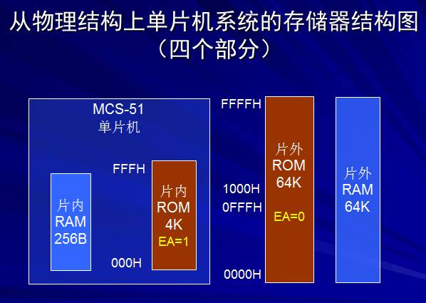
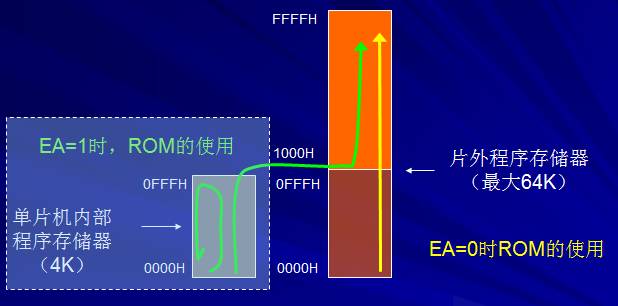
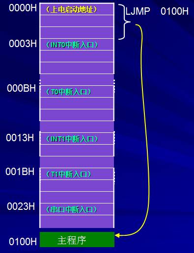
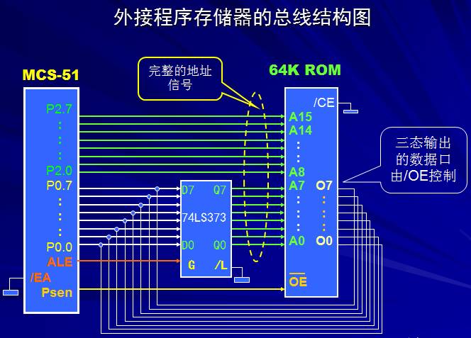
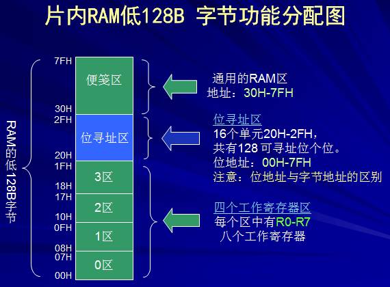
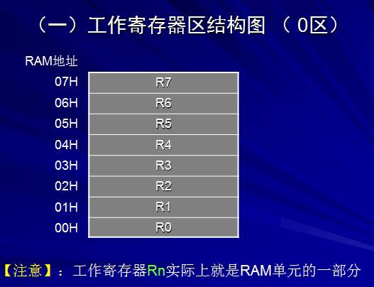
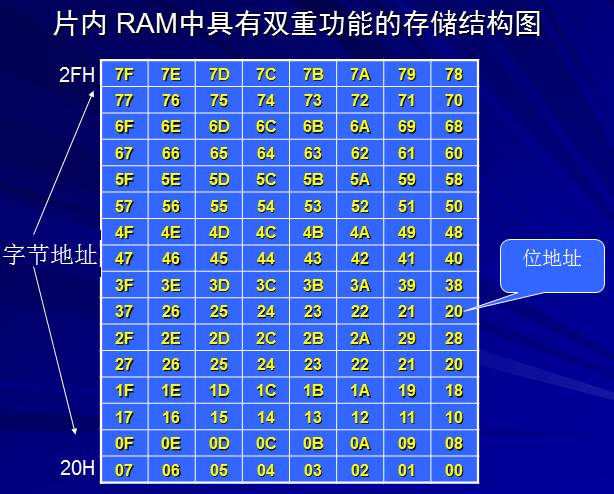
1. An 8-bit microprocessor CPU. 2. On-chip data memory (RAM128B/256B): used to store data that can be read/written, such as intermediate results of operations, final results, and data to be displayed. 3, on-chip 4kB program memory Flash ROM (4KB): used to store programs, some raw data and tables. 4. Four 8-bit parallel I/O (input/output) interfaces P0~P3: Each port can be used as an input or as an output. 5, two or three timer / counter: Each timer / counter can be set to the counting mode, used to count external events, can also be set to the timing mode, and can achieve computer control based on the results of counting or timing 6, a full-duplex UART serial I / O port: can achieve serial communication between the microcontroller and the microcontroller or other microcomputer. 7, on-chip oscillator and clock generation circuit: but need to external crystal and capacitor. 8. Interrupt control system for five interrupt sources. 9, with power-saving work: leisure and power-down. In the idle mode, the CPU stops working and the RAM, timer/counter, serial port, and interrupt system continue to operate. The current at this point can be reduced to approximately 15% of the normal mode of operation. In the power-down mode, the on-chip oscillator stops working. Since the clock is "frozen", all functions are suspended, so only the contents of the on-chip RAM are saved until the next hardware reset. The current in this mode can be reduced to less than 15 μA and the minimum can be reduced to 0î€6 μA. structure: It consists of a central processing unit (CPU), memory (ROM and RAM), and an I/O interface. The internal structure of the 89C51 microcontroller is shown in the figure: Introduced below is mcs-51 MCS-51 microcontroller memory configuration features 1 Internally integrated 4K program memory ROM; 2 internal with 256B of data memory RAM; 3 You can externally connect 64K of program memory ROM and data memory RAM. From the perspective of physical structure, the 51 MCU storage system can be divided into four storage spaces: on-chip ROM, RAM and off-chip ROM, RAM. Logically speaking (from a programming perspective), the 51 MCU storage system is actually divided into three storage spaces. 1. On-chip data memory RAM; 2. Off-chip data memory RAM; 3. On-chip or external program memory ROM (determined by EA level). 1. Program memory ROM is used to store programs, constants or tables. 2. In the 51 MCU, the internal and external ROMs are selected by the level on the pin / EA: When EA=1, the CPU executes the program in the on-chip 4KROM; when EA=0, the CPU selects the program in the off-chip ROM. . 3. Whether using on-chip or off-chip ROM, the starting address of the program starts from the 0000H unit of the ROM. 4. Although the system can have both on-chip ROM and external ROM, in normal use, select one by using /EA (or use internal ROM, or use external ROM). 5. If EA=1 (when executing the program in the on-chip program memory): If the PC value of the program counter pointer exceeds 0FFFH (4K), the microcontroller will automatically switch to the off-chip ROM memory and execute the program from the 1000H unit ( Unable to use the low 4K space of the off-chip ROM). 6. When the program exceeds 4K, there are two ways to use the program memory ROM: 1 Set EA=0 to use the external ROM. Starting at address =0000H; 2 Set EA=1, use the internal 4KROM and external ROM (units starting from 1000H). Program memory six special units: There are six units in the ROM with specific functions. 0000H unit: the unit pointed to by the program counter PC during reset, so it is used to store the first instruction in the program; 0003H unit: vector interrupt address of external interrupt / INT0; 000BH unit: vector entry address of timer T0 overflow interrupt; 0013H unit: vector interrupt address of external interrupt / INT1; 001BH unit: overflow interrupt vector entry address of timer T1; 0023H unit: Interrupt vector entry address for serial port reception and transmission. Vector entry unit: When writing an interrupt program, write the corresponding "springboard instruction" Two features of the first instruction of the microcontroller: 1 stored in the 0000H unit of the ROM; 2 must be a "jump instruction" to skip the following 5 interrupt vectors, and go to the real main program entry 0100H unit. ORG 0000H LJMP 0100H ORG 0100H START: MOV A, #00H : : : : : : : : END When the MCU uses the external ROM memory (extended system), /EA=0 must be set. At this time, the port function of the MCU will change accordingly: 1 P0, P2 as the address and data bus of the external ROM; 2 Use the pin /psen signal to gate the data tristate output of the external ROM. Whether physically or logically, the RAM in the system can be divided into two separate spaces: internal and external RAM. Accessed by different instructions. 1. Use the MOV instruction when accessing the internal data storage unit; 2. Use the MOVX instruction when accessing the external data memory. The internal RAM functionally divides the 256B space into two different blocks: 1. Low 128B RAM block; 2. A 128B SFR (Special Function Register) block. In the low 128B RAM memory unit, it can be further divided into: 1. Working register area; 2. Bit addressing area; 3. "Note area" for general storage data. Only the 21 registers (51 series) are used in the special register area SFR of the high 128B, and the other 107 units cannot be used.
Rectangular I/O Connectors
Antenk develop and specify high-performance I/O's throughout a wide variety of industries. These include SAS, SATA, PCIe, HSSG, FIBRE CHANNEL, INFINIBAND, IEC, CEA, IEEE, VESA, USB and many more.
I/O Connectors Application
Antenk can deliver standard and custom options of the following I/O connectors:
I/O Connectors General Specifications
ELECTRICAL CHARACTERISTICS
Rectangular Connector,Rectangular I Connectors,Rectangular O Connectors,Male Connector Rectangular,I/O Connectors,Input/Output Connectors ShenZhen Antenk Electronics Co,Ltd , https://www.pcbsocket.com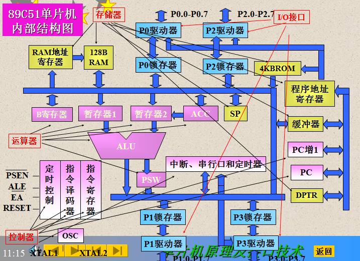

Antenk offers an expansive product line of I/O connectors including USB, HDMI, D-Sub, Modular Jacks, SFP, QSFP+, CXP, iPass+, iPass+ HD and more. In addition to standard I/O connectors and matching cable assemblies.Except a comprehensive range of standard Input/Output connector solutions for high-speed electronic data communication, Antenk engineers can design customized solutions. This extensive selection of I/O connectors and matching cable assemblies includes numerous next-generation solutions.All of our I/O connectors feature a variety of orientation options, as well as PCB and cable mount offerings.
Consumer / PC Products
Networking / Telecommunications Products
Mobile Products
Industrial Products
1394 Connector
Centronic Connector
D-Sub Connector
DVI Connector
Display Port Connector
HDMI Connector
Half Pitch SCSI Connectors
USB Connector
V.35 Connector
OBD Connector


Contact Current Rating:5Amperes.
Dielectric Withstanding.
Dielectric Withstanding Voltage:AC 1000Vr.m.s.
Insulation Resistance:500 Megohms Minimum at DC500V.
Contact Resistance:25 Milliohms Maximum.
Operating Temperature:-55℃~105℃.
")
MATERIALS:
Contacts:Brass.
Insulator:PBT,UL94V-O Rated.
Shell:Cold Rolle Steel.
Metal Watertight Frame:PBT,UL94V-0.
O-Ring:Silicone.
NOTE:
Position:09PIN,15PIN,25PIN,37PIN.