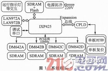
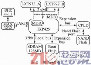
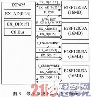
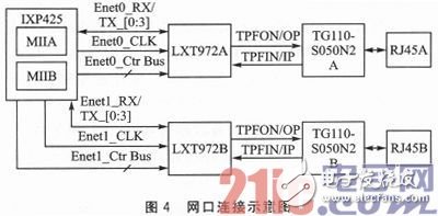
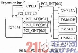
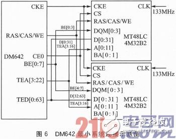
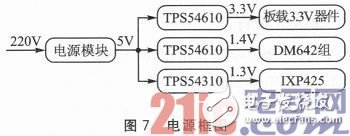
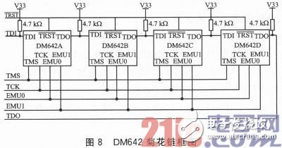
This paper introduces the hardware design principle and implementation method of conference TV multi-point control unit using IXP425 as the core main control unit and 3 DM642 as the core data processing unit. The main controller IXP425 module completes functions such as network transmission/reception, data scheduling, and PCI control. The data processing DM642 module performs functions such as audio/video mixing and switching. The PCI bus is connected between IXP425 and DM642, and the data transmission speed between each module is fast, which improves the data processing efficiency. "Conference TV system" refers to people or groups in different places, through the communication lines and multimedia communication equipment, to transmit sound, video and text materials to each other to achieve instant and interactive communication, thus achieving the completion of traditional centralized conferences. The system of purpose. By means of conference TV, participants in multiple venues can hear the voices of other venue personnel and see images of other venues. Participants can express their opinions and observe through audio/video transmission communication. The other party's image, in addition to the physical objects, drawings, etc. to enhance the sense of the scene, you can also send relevant documents, charts or discussion questions in a timely manner by fax or share the electronic whiteboard, etc., shorten the space distance between the participants, improve the atmosphere of the meeting, and make the meeting People can be immersed, just like meeting in one place. The conference television system is mainly composed of a terminal device, a transmission channel (communication network), and a MCU (MulTIpoint Control Unit). Among them, the multi-point control unit is the core part of the conference television system, and its function is equivalent to the switch in the computer network. The switch extracts the information, signaling, and other information, such as audio, video, and data, from the information flow of each conference site, and then sends the information and signaling of the conference site to each processing module to complete the corresponding tone/ The process of video mixing or switching, data broadcasting and routing, timing and conference control, and finally reassembling the various information required for the meeting place and sending them to the conference television terminals. This paper is based on the design of a low cost, stable operation, full function, large capacity, fast computing speed, good compatibility, good security, simple operation, and can run under 2M network bandwidth for small and medium-sized The user's embedded conference TV multipoint control unit. The main functions of the Conference Television Multipoint Control Unit (MCU) are: 1 media control, media processing: including audio and video extraction, audio and video re-encoding, mixing, switching, etc., data broadcasting and routing, voice excitation calculations and other required media functions; 2 can receive audio and video data forwarded by other multi-point control units, re-sound/video switch or mix and send to the conference TV terminal for decompression decoding, restore to sound, video and computer data for local output; The 3MCU and the terminal follow a protocol (such as H.323, SIP, etc.) to connect; The 4MCU and the terminal can receive and respond to the control signal sent by the other party; 5 network access function; 6 Parameter settings can be made via RS232. 1 program design Solution 1: The implementation of a multi-point control unit in a desktop video conferencing system based on TCP/IP protocol is proposed in the reference. The scheme adopts a pure software structure, the scheme cost is low, and the development cycle is short, but the scheme processes the sound. The number of video channels is limited and the picture quality is poor. Option 2: A DSP-642 based conference TV hardware platform solution is proposed in the reference, which is designed and implemented based on H. The 264 protocol pixel domain multi-picture synthesis PCI communication module, video codec module, but the capacity is only 4 channels, the picture quality is general. Comprehensive comparison of the above two schemes, combined with the specific situation of the MCU of the conference multi-point control unit, the conference TV multi-point control unit MCU designed by Intel uses the Intel embedded processor IXP425 as the main controller and uses 4 DM642 chips as data processing. The chip, the main controller and the data processing module use a PCI bus for communication. This kind of solution development cycle is relatively short. TI, InteI and other chip manufacturers provide a complete software and hardware development package. In addition, the PCI bus is used to connect the main controller module and the data processor module, and the data transmission speed is fast and the throughput rate is high. 2 system design The system block diagram and the function chip used are shown in Figure 1. The system is mainly composed of a control module and an audio/video processing module. The control module consists of the IXP425+CPLD on the board. Responsible for the resource and information management of the board, and forward the audio/video signals sent from the service board to the corresponding DM642 for processing. The board's CPLD mainly implements functions such as resetting, clock detection, chip select signal control, register reading and writing, and board information. The audio/video processing module is completed by four DM642s on the board and is the core module of the board. There are two key factors that determine the performance of an audio/video processing module: the audio/video algorithm performance and the transmission performance of the PCI bus. In order to enhance the transmission performance of the PCI bus, it can be improved from the following two aspects: improving the transmission efficiency of the PCI bus; any device on the PCI bus can be transmitted as a master device, so that data transmission between the DSP chips is not forwarded through the IXP425, saving Bus bandwidth. 2.1 IXP425 module The IXP425 module mainly includes a CPU minimum system, a CPLD control module, a debugging module, and a network management module. The block diagram is shown in Figure 2. IXP425 itself has an Expansion bus, which enables flash, HPI bus devices, SDRAM and other devices to be connected to the internal ASHB. It is compatible with Intel/Motorola and other standard interfaces. There are 8 bank selections of cs[7:0], each block size is 16 MB, if using WinCE operating system, the Flash space is at least 20 MB or more, so the minimum system design uses two banks of cs0 and cs1 as the system storage space. In order to leave enough storage space for the program download mode, two 16 MB of Flash were added. The Flash connection is shown in Figure 3. Because the IXP425 has a dedicated SDRAM controller built in, according to its interface principle, and considering that the platform has a certain margin for computing performance, the minimum SDRAM part of the system is designed with two 32 MB SDRAMs, and the hardware is compatible with 128 MB. SDRAM design. 2.2 Network port design The IXP425 has three network processor NPEs working in parallel with the XScale core. It can provide two MII interfaces to the outside. The principle of parallel operation makes the network processing performance better. It supports 802.3 protocol content. The standard MII interface only needs to be externally connected. PHY physical interface chip, the platform uses Intel's LXT972A, which can complete the interaction with external data. Of course, the use of the transformer is also necessary, using the TG110-S050N2 produced by HALO and the RJ45 interface, the connection diagram is shown in Figure 4. Since the IXP425 has a built-in MAC controller, the sophisticated MII interface makes the platform's network application simple and targeted. 2.3 audio / video processing module design 2.3.1 PCI interface design The IXP425 PCI controller has four DM642s externally connected, and the bus is 33MHz. The connection diagram is shown in Figure 5. IXP425 PCI bus mainly completes boot load, chip configuration management, PCI bus arbitration and media stream scheduling for DM642. The DM642 chipset mainly performs the functions of encoding and audio/video synthesis of audio/video media streams. The current capacity is 4 channels of audio/video synthesis, and the video algorithm is H. 264, the speech algorithm is AAC, G. 723.1 and so on. Among them, DM642A occupies PCI slot 1 of IXP425, DM642B occupies PCI slot 2 of IXP425, DM642C occupies PCI slot 3 of IXP425, DM642D occupies PCI slot 4 of IXP425, and its corresponding corresponding pin interconnection is as follows: DM642A Corresponds to the PCI pin of the IXP425. The PCI interrupt control signal is reported to the CPU by the CPLD, and the CPU determines the interrupt event of the peripheral PCI device by reading the interrupt register inside the CPLD. 2.3.2 Minimum system design for audio/video processing module EMIFA allows seamless connection of multiple SDRAMs. Since the selected SDRAM size is 64 MB, the DM642 minimum system is shown in Figure 6 according to the DM642 EMIFA interface guidelines. The chip selection is completed by CE0. After two 16MB SDRAMs are used for bit expansion, the maximum address space is 32MB, the row address strobe is A[3:10], and the column address strobe is A[3:14]. The bankselect is A[15:16], so the DM642 address line A[3:16] is used. The DM642 core operates in 50M & TImes; 12 Hz mode, the EMIF interface operates at 25M x 5.33 Hz, and the PCI interface operates at 33 MHz clock frequency. 2.3.3 Flash design IXP425 plugs a piece of Flash and stores the BOOT program. After the chip is booted, import the image of the IXP425 from the large-capacity Flash into the memory. The DSP program does not separately configure the flash memory, and the IXP425 imports the DSP program into its own RAM through the PCI bus. IXP425 is the master of the PCI bus, and other DSP chips are slaves. The process of IXP425 booting the DSP through the PCI bus is as follows: 1DSP configuration pin is set to PCI BOOT mode (AEA[22:21]=01, [PCI_EN:TOUT0/MAC_EN]=10) 2IXP425 releases the reset pin of DM642 through CPLD, and DM642 enters the installation state; The 3IXP425 configures the PCI register of the DM642 through the PCI bus; 4IXP425 sets the memory and I/O space of the DM642; 5IXP425 imports the BOOT program of DM642 into the internal RAM of DM642, the starting address is 0; The 6IXP425 accesses the memory space of the DM642 and writes the program into the memory of the DM642. The page register (DSPP) of the DM642 allows the IXP425 to access all the space of the DM642. 7IXP425 sets the DSPINT bit of the HDCR register of the DM642 to 1, releasing the DM642 from the installed state; The 8DM642 starts the BOOT program from address 0. 2.3.4 OPLD design The specific functions of the board's CPLD are as follows: board IC reset control, interrupt processing, clock detection, clock division, clock timing (clock synchronization), chip select decoding, and I/O expansion. The board uses a CPLD and CPLD resources. The requirement can only be used up to 70%, and the future is upgraded and the wiring is tight. 2.4 Clock Design (1) PCI clock The output of the 33 MHz crystal oscillator is divided into 8 channels after a BUF: the CPLD is used as the detection clock; the OSC-IN of the IXP425 is used as the chip operation clock; the EX_CLK pin of the IXP425 is used as the Expansion bus clock; the IXP425 is all the way to the IXP425. PCI, as the clock of PCI; the remaining 4 channels are sent to the PCI clock driver. (2) Ethernet and SDRAM clock The 50 MHz crystal oscillator is used as the main clock of the CPLD. After the clock is divided by 2, it is sent to each Ethernet chip as the master clock of the respective chip, and each clock has no synchronization requirement. The DM642 SDRAM clock is acquired by the ICS512 multiplier, while the IXP425's SDCLK_OUT has a strong drive capability and directly drives four SDRAMs. 2.5 Single Board Power Supply Design The power supply block diagram is shown in Figure 7. 2.6 JTAG link The JTAG of the single-board CPU and CPLD are separately chained for easy loading and debugging. Four DM642s are connected into one daisy chain, and the hardware is compatible with each chip for separate debugging. The daisy chain block diagram is shown in Figure 8. 3 hardware debugging The hardware part of the multipoint control unit mainly performs the following debugging: 1 Power supply, reset module debugging: solder power module chip and peripheral circuit, test +5 V, 3.3 V, 1.4 V, 1.3 V voltage output is normal. After the voltage output is normal, solder the reset circuit components. After power-on, observe whether the reset voltage and the duration meet the design requirements. Use the oscilloscope to measure whether the level and duration of the reset signal match the design. After power-on, pay attention to whether each voltage conversion chip is hot. If it is not normal, immediately turn off the power to check. 2 minimum system debugging: soldering IXP425 chip, DM642 chip, CPLD, SDRAM, Flash, JTAG interface and peripheral components of each module on the board. Use an amplifier to carefully check for short circuits, open circuits, solder joints, solder joints, and false solder joints. Power on after no problem, measure the working voltage of each chip is normal, use oscilloscope and frequency meter to measure whether the working clock of each module is normal. Use the JTAG port to connect the hardware to the computer. After configuring the control registers, test whether the SDRAM read/write function is normal, and whether the Flash erasing function is normal. If the work is not working properly, check the timing signal, hardware connection, etc. 3PCI bus debugging: test whether the data transmission between each function module is normal, such as IXP425 read and write 4 DM642, D642 read and write data, etc., need to be combined with computer, oscilloscope, spectrum analyzer, logic analyzer, etc. 4 network transceiver module debugging: welding LTX972A and peripheral devices. Check whether the connection between the MII interface of the IXP425 and the LTX972A chip is normal. Test whether the network transceiver module can communicate with the local PC through the network port through the LTX972A test program provided by Intel. 4 Conclusion The multi-point control unit has the following features in design: 1 non-PC embedded conference TV multi-point control unit design; 2 The internal PCI bus connection is used to solve the problem of large burst of data transmission and synchronization of each data processing module in the multi-point control unit of the conference television; 3 multi-parallel data processing module design. COB Light
COB LED par light for theatre, productions, TV studio, stage
Description:
COB200-2in1 is a professional theatre fixture that utilizes a 200W warm-white and cold-white COB LED with a color temperature of 3200k-6000K. Users are able to creat a customized color tempreature via a DMX Controller or set directly on the display menu. It offers a high-power light output with rich hues and smooth color mixing for stage and wall washing. The double bracket makes installing easily and versatile.
Our company have 13 years experience of LED Display and Stage Lights , our company mainly produce Indoor Rental LED Display, Outdoor Rental LED Display, Transparent LED Display,Indoor Fixed Indoor LED Display, Outdoor Fixed LED Display, Poster LED Display , Dance LED Display ... In additional, we also produce stage lights, such as beam lights Series, moving head lights Series, LED Par Light Series and son on...
COB Light Series,Led Par Light,54 Led Par Light,Par Led Lights Guangzhou Chengwen Photoelectric Technology co.,ltd , https://www.cwstagelight.com