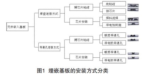
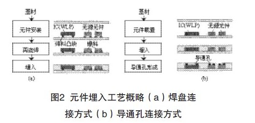
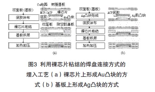
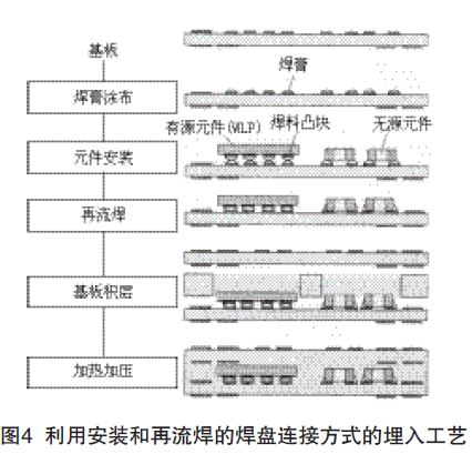
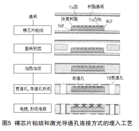
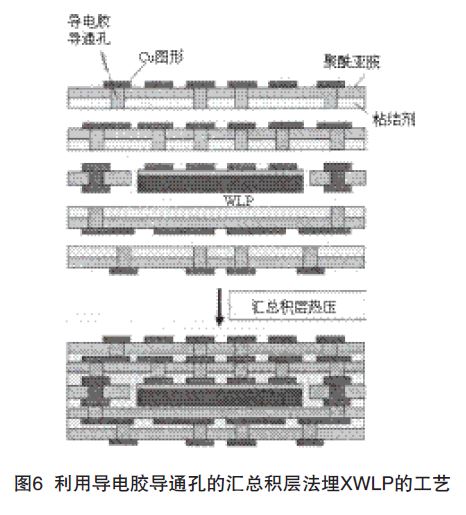
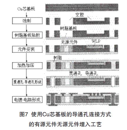
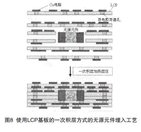
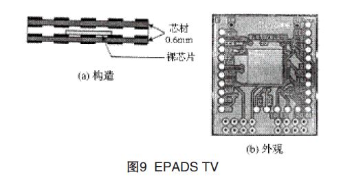
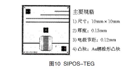
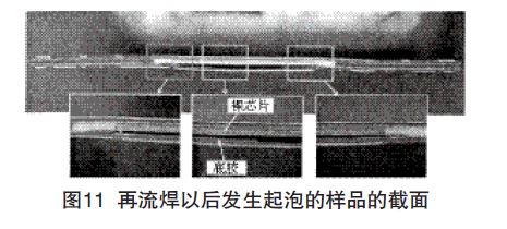
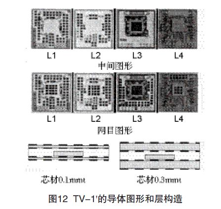
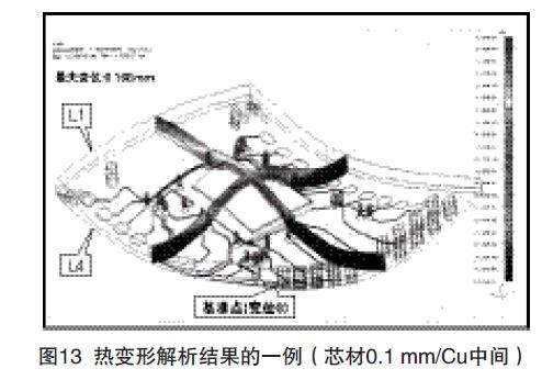
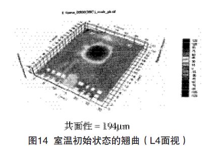
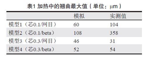
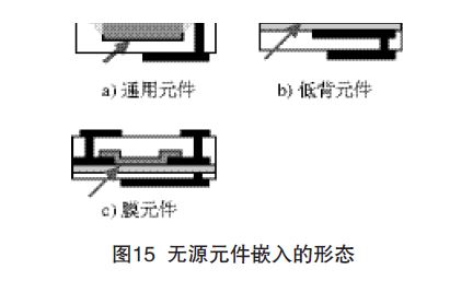
The embedding of the element substrate allows the PCB or module to be miniaturized due to the three-dimensional arrangement of the components, shortens the connection path between the elements, and reduces the transmission loss. It is an installation technology that can realize the multifunctional and high performance of the portable electronic device. In view of this, this article mainly summarizes the component interconnection technology of the buried component PCB and the evaluation and analysis of the buried component PCB. 1 Introduction The embedding of the element substrate allows the PCB or module to be miniaturized due to the three-dimensional arrangement of the components, shortens the connection path between the elements, and reduces the transmission loss. It is an installation technology that can realize the multifunctional and high performance of the portable electronic device. Embeded-substrate substrates embedding LSIs or passive devices in multilayer boards have been used since 2003. Since 2006, they have been officially used as high-performance mobile phones or small-module substrates for watch applications. These substrates employ the unique features and processes independently developed by component manufacturers and PCB manufacturers, respectively. In this paper, the classification of buried-substrate substrate technology embedded in the specifications of the Japanese Electronic Circuit Industry Association (JPCA), the components used, the mounting technology, and evaluation analysis are introduced. 2 Classification of buried component substrate technology The embedded device substrate is roughly divided into a mode of embedding individually manufactured components and a mode of forming a direct component on a substrate. I am limited to the former method of technology. FIG. 1 shows a classification of a buried type embedded device substrate according to an embedded device mounting method. There are two types of component mounting on the PCB: pad connection and via connection. FIG. 2 shows a representative manufacturing process of a pad connection method and a via connection method. In the pad connection method, first, an embedded element is mounted on an electrode formed on a substrate and electrically connected. After the connection is completed, the insulating resin is used to simultaneously fill and bury the components and electrodes. Use existing surface mount technology when connecting. The connection material is made of solder or conductive adhesive. Installation of embedded components: Die bonding is used when the component is bare die; Mounting is used when the component is passive component or Mould Package or WLP (Wafer Level Chip Scale Package). Flip Chip Bond uses ultrasonic bonding, C4 (Controlled Collapse Chip Connection), ESC (Epoxy Encapsulated Solder Connection), conductive resin, and anisotropic conductive resin (ACF) /ACP, Auisotropic Conducive Film/Anisoropic Conductive Paste), and non-conductive resin (NCF/NCP, Non Conductive Film / Non Condctive Paste). Passive components are connected using solder reflow or conductive resin. The pad connection method has the advantage of using existing manufacturing equipment effectively because the component connection uses conventional surface mounting technology. In addition, since the inspection after the component mounting connection is performed and before the embedment is performed, it is possible to screen, repair, and rework the defective product that occurred during the mounting process. In the through-hole connection method, an insulating resin is buried in the element before the electrical connection between the PCB and the element. After the component is buried, laser processing is performed on the resin covering the element electrode, and after the via hole is formed, the plating is used to fill the via hole to electrically connect the PCB and the element. Via connections are characterized by direct copper (Cu) plating on the electrodes of the device. Since there is no joint such as solder or bumps used in surface mounting, low connection resistance and high connection reliability equivalent to the internal wiring of the multilayer board are expected, and a full-layer IVH (Interstitial Via Hole) can also be used. The conductive adhesive is used for via connection, and the same conductive adhesive as the interlayer connection of the multilayer board is used for connection with the components. The integrated build-up process that simultaneously performs embedding and connection can simplify the assembly of the component with a complicated structure. The manufacturing process. The types and general manufacturing processes of the buried element substrates classified according to the mounting technology of the buried components have been described above. In the following, various mounting techniques used in the manufacture of a buried component substrate will be described with reference to the examples of development to date. 3 pad connection embedded device substrate In the pad connection method, after the components are mounted on the inner substrate, the insulating resin is embedded. The embedded components are divided into Bare Dies and other components. The surface mounting technology for connection is described below. 3.1 bare die bonding Figure 3 shows the process of inserting a bare chip using flip chip mounting. FIG. 3(a) shows that gold (Au) build-up bumps are formed on the bare chip electrodes. Use NCP and PCB electrodes for heating and pressure connection. The surface of the electrode of the PCB is not plated with gold (Au) or tin (Sn), but is originally copper (Cu). The copper (Cu) surface is roughened to improve its adhesion to the resin. In the heating and pressurizing connection, the joint must maintain the compressive stress, which is important for improving the connection reliability. In Fig. 3(a), focusing on the thermo-mechanical properties of NCP, a highly practical and reliable connection reliability can be obtained by selecting a resin with high elasticity and high expansion coefficient. There is also a method of installing a thermocompression connection using ACP instead of NCP. After a gold (Au) ball bump is formed on a bare aluminum (Al) electrode, the primer ACP is applied and pressurized and heated to electrically connect. Bonding reliability with NCP also depends on the physical properties of the primer resin. Figure 3(b) shows the connection using silver (Ag) adhesive bumps and ACP. A silver (Ag) paste is printed on the electrode of the PCB to form silver (Ag) bumps, and the coating primer ACP is heat-press bonded using a chip-bonding device. No copper (Cu) or gold (Au) bumps are formed on the electrodes of the bare chip, but aluminum (Al) is used for the thermocompression bonding. The bonding technique of the thermally-pressed silver (Ag) adhesive bumps of FIG. 3(b) has been mass-produced in a build-up board, and it is an application of an interlayer connection technique using a conductive bump (B2it, Buried Bump Interconnection Technology). . 3(a) and 3(b) are practical components of the device-embedded substrate combined with the multi-layer board manufacturing technology. The connection of layers is performed using conductive bumps using the component connection technology of NCP and ACP. A double panel made of conductive resin bumps is manufactured. After the components are mounted on the inner layer, the components are assembled together with the outer layer of the substrate under heat and pressure to embed the components, and the bumps are used to collectively connect the circuit layers. The process of forming a line prior to the embedding of the element is advantageous in reducing the defective rate and improving the productivity. 3.2 Chip Installation FIG. 4 shows a connection method in which a chip mounter is mounted on a substrate of an inner layer of a printed solder paste and the solder is melted using a reflow process. The mounting and connection of the active element and the passive element are performed simultaneously with the chip mounting and the reflow process for LSI WLP. It is an embedded technology that can be used for most common components such as model-packaged LSIs or modules. When the embedded component is soldered, since the module substrate on which the component is mounted on the surface of the substrate is mounted on the mother board for the second time, there is a fear that the solder bump (solder ball) melts and influences the conduction and insulation characteristics during the reflow process. . Therefore, the periphery of the solder is covered with the resin, and the flow caused by the remelting is suppressed, so that the above problem can be avoided. 4 via hole connection element embedded substrate In the via hole connection method, after the component is embedded, it is connected to the substrate. The electrodes of all the elements of the active element and the passive element are regarded as an inner-layer wiring pattern, and a wiring layer is formed on the upper part of the element by a build-up technique. 4.1 bare die bonding The embedded LSI WLP technology uses copper (Cu) lines to draw out WLP-based electrodes, increasing the pitch between the electrodes, and achieving a high-affinity embedded process with the existing PCB processing technology. In addition, a good bare chip (KGD, Known Good Die) is secured due to WLP. This is a great advantage compared to the through-hole connection where it is difficult to repair components after connection. FIG. 5 shows a manufacturing process of a typical via-connection active element embedding technique. Embedded LSI WLPs form copper (Cu) lines and copper (Cu) bumps for resin coating. After affixing a die attach film (DAF, DieAttachment Film) on the back surface of the thinned chip, the positions are overlapped and bonded to the top surface of the substrate. The prepreg and the surface substrate are laminated, and the bare chip is embedded after heating and pressing. Laser processing is performed on the surface of the embedded WLP electrode from the surface of the substrate to form a via hole, and a plating layer is used to fill the via hole to connect the WLP electrode and the circuit of the substrate. Because the surface of the bare chip is protected by the resin, it is possible to reduce the risk of damage or contamination in the embedded process engineering. FIG. 6 shows a method of using a conductive paste for the material of the via hole. The copper (Cu), silver (Ag), and sintered alloy materials used for the interlayer connection of the multilayer board are connected by crimping or metal bonding. FIG. 6 shows an example of WLP embedded in a polyimide multilayer board and thinned by back grinding. The embedded LSI is WLP-processed to increase the pitch of the electrodes to the same pitch as the PCB vias, and the thickness is reduced to 0.1 mm or less. Vias formed on the substrate are filled with uncured conductive paste, and the substrate/WLP and the spacer/substrate are laminated and heated and pressurized once. During the heating process, the conductive paste filled in the via hole is solidified, the flow and curing of the bonding material are sequentially performed, and the electrical connection and the embedded bonding between the PCB/WLP are completed at the same time. In the one-step build-up method using a conductive adhesive via hole, since a full-layer wiring has been formed before the build-up of the PCB and the embedding of elements, there is an advantage of reducing the defective rate that occurs after component insertion. In order to adapt this process to future multi-pinning of LSIs, miniaturization of via pitches connected to bare chips is a problem in the future. 4.2 Mounting Mode Figure 7 shows the component embedding process using laser vias and plating connections. The embedded component is placed in a cavity provided on a part of the substrate and then filled with resin to embed the component. Using a thick copper (Cu) core substrate, a cavity is formed by etching of copper (Cu). A resin sheet is attached to one side of the core board, and after blocking one side of the cavity, the component is fixed on its bottom surface. A resin sheet is laminated on the opening side of the cavity and heated, and the gap between the inner wall of the cavity and the element is filled with resin to fix the element. The resin embedded in the electrode of the element forms a laser via opening. A semi-additive method is used to form the surface layer circuit of the substrate while a through-hole is filled with a copper (Cu) layer. The connection of the front and back sides of the substrate is opened at a part of the copper (Cu) core in advance when the cavity is formed, and the through hole is formed by laser after the resin is filled. Substrates using this technology have excellent thermal conductivity, and especially feature high heat dissipation when embedded in a device that generates a large amount of heat. FIG. 8 shows a conceptual diagram of an element embedding process using a single-layer method. As a passive element embedding technique using a primary laminate method using a conductive adhesive, an Ag-Sn alloy material is used for via holes, and LCP is used for insulation. material. The number of single-layer laminates that form the cavity at the component is specified, and at the same time, the component is heated and pressurized after it is inserted into the cavity. The glue material composed of Ag and Sn filled in the via hole is sintered due to heating, and at the same time Sn diffuses to the wiring board and the Cu electrode of the element to form a metal bond. The thermoplastic material LCP (Liquid Crystal Polymer) softens due to heating, bonds the substrates together, and at the same time flows into the gap between the device and the cavity to be embedded in the device. In the heating and pressurizing process, since the flow of the resin affects the formation of the via hole, and there is a via hole near the gap between the element and the small substrate, the precise control of the resin flow is essential to ensure the connection reliability. 5 embedded components In the pad connection mode, most components embedded in the surface mount technology such as reflow or adhesive can be used. In order to avoid an extreme increase in the plate thickness, components having a small element thickness are used. In the case of bare chips or WLP, most of them grind the back surface of silicon (Si), and the height after mounting (including recesses) is (300 to 150) mm or less. Passive components using 0603-type, 0402-type or 1005 low-back type. When the through-hole connection method is adopted, the above-described examples of the plating connection and the connection of the conductive adhesive are all elements using a Cu electrode. The use of a passive element thickness of 150 mm for a copper (Cu) electrode as an embedded element is one of the goals, and there are development examples for thinner elements. 6EPASD Evaluation Analysis TV (TestVehicle) 6.1 Test Vehicle (TV) Overview For the purpose of elucidating the technical problems in which the components are embedded in the PCB, a TV (Test Vehicle) in the evaluation analysis WG was produced and evaluated. From the discussion of construction and design again in 2007, a bare chip embedded substrate structure as shown in FIG. 9 was finally produced. The circuit layer is 4 layers, and components are embedded between L2 and L3. According to the purpose of component embedding in the PCB, the initial comment should be the same as that of the HDI substrate, and it is considered that the problems unique to device embedding are regarded as the most fundamental problems. It is extremely easy to manufacture with the exception of the embedding portion, and the interlayer connection is a through hole. Manufactured using halogen-free FR-4 and FR-5 substrates, respectively. The embedded element is "SIPOSTEG" provided by SIPO (System Integration Platform Organization Standard) and forms a pad configuration such as a daisy-chain pattern connected to the PCB. Figure 10 shows this pattern and main specifications. The gold (Au) stud bumps (Stud Bump) are formed on the electrodes, and the face-down flip chip connection is adopted. At this time, two methods of thermocompression bonding and ultrasonic methods were used. Therefore, a total of four kinds of samples of two kinds of materials and two kinds of mounting methods were prepared. 6.2 Evaluation Results TV production was implemented in 2008, and evaluation analysis was conducted in 2009. First of all, in order to evaluate the reflow heat resistance, the pretreatment was carried out using JEDEC grade 3 conditions. Foaming occurs after many samples are reflowed. In addition, it is accompanied by the occurrence of disconnection or resistance increase. FIG. 11 shows an example of cross-section analysis. Peeling occurs between the underfill resin and the chip under the embedded chip, and part of the peeling occurs at the interface between the bolt-shaped bump and the PCB electrode. This peeling is the cause of blistering. Several blisters also occurred in the heat-resistant FR-5. There are no significant differences among the four conditions. Therefore, the main reason for the occurrence of foaming is the structure itself. According to the result of the cross-section analysis, the chip itself is significantly warped, and since the residual stress inherent in the embedding is released when reflowing, it is deformed, or due to the size of the chip itself or the influence of the PCB pattern. Regarding the warpage, the convex warp was exhibited due to the difference in thermal expansion coefficient between the chip and the inner layer when mounted on the inner layer plate, but the concave area was reversed to the concave warp shape in the section after foaming as shown in FIG. 11 . It is worth noting. The evaluation of the occurrence of blistering is essentially due to Popcorn phenomenon. The same blistering has been found with different installation methods of the two base resins. Therefore, it is considered that the PCB structure has a great influence. In order to investigate this phenomenon, a TV-1' core material having a thickness of 0.1 mm and 0.3 mm was fabricated for the second time. The copper pattern (Cu) of the conductor pattern and the mesh of the PCB were used for the TV-1 (Mesh). There are two types of graphics. A total of four samples. Figure 12 shows the conductor pattern and layer configuration of the TV-1' PCB. In each structure, five reflow heat resistance tests were carried out, and a blistering phenomenon was reproduced in the 0.1 mm/Cu intermediate pattern of the core material in the same structure as that of the TV-1′. No blistering or resistance increase occurred in other structures, and the structure was confirmed. The effect of the change. 6.3 Analysis of Thermal Deformation In order to examine the influence of the thickness of the substrate or the line conductor pattern on the thermal deformation behavior of the element embedded in the PCB, the results of the simulation obtained so far were analyzed. According to the Geber data of the EPADS TV described in the previous section, a three-dimensional model (Model) was prepared and analyzed by analyzing the thermal deformation behavior from room temperature to 260°C. In the analysis, nonlinear elastic analysis was performed using ADINA 8.6 (manufactured by ADINA Corporation, USA). The analysis is based on TV-1'. The thickness of the substrate is 0.1 mm and 0.3 mm, and the conductors of the PCB are set to two kinds of copper (Cu) intermediate patterns and mesh patterns, and a total of four types of analysis are performed. The model made is as follows. (a) Model 1 core 0.1 mm thick/mesh pattern. (b) Model 2 core material 0.1 mm thick / middle pattern. (c) Model 3 core 0.3 mm thick/mesh pattern. (d) Model 4 core material 0.3 mm thick / middle pattern. In addition, the embedded chip is 0.1 mm in thickness and 10 mm in thickness, and the same peripheral gold (Au) bumps and bottom underfill resin structure are configured as in the TV. The actual manufacturing conditions are different. In the analysis, the stress and deformation at room temperature are set to 0, and the thermal behavior at heating to 260°C is obtained. An example of the thermal deformation analysis result is shown in FIG. The PCB L1 on the way indicates the above, and the central portion of the bare chip embedded portion tends to deform in a convex shape. It is surrounded by the deformation of the embedded part of the bare core. Deformation behavior varies from site to site due to the shape and density of the conductor pattern. Analyze the four models. Model 2 corresponds to a structure in which TV-1 foams. The amount of thermal deformation obtained by the analysis was the largest in the model 2 and showed the same tendency as the actual substrate. The deformation of Model 2 is 108 mm, and that of other models is 46 mm to 60 mm. 6.4 Comparison with Thermal Deformation Measurement In order to verify the accuracy of thermal deformation analysis, actual measurement of thermal deformation behavior was performed. The sample was manufactured as TV-1', and a model 1 to model 4 of considerable thermal deformation analysis was supplied for the test. The measurement was performed while heating up to 260°C according to the non-contact warpage measurement of the Shadow Moire method. Figure 14 shows the warpage distribution in the initial state at room temperature. Contrary to the analysis result, since the L4 side has a convex warpage, the PCB L4 is disposed thereon. Since this warpage direction corresponds to the direction of warpage of the chip after foaming shown in FIG. 11, the chip is embedded and mounted. Shows different warping. From the initial state of the room temperature to 260°C, several points were measured while the temperature was raised, and it was confirmed that the warpage at the initial state of the room temperature was small, that is, the warpage behavior was exhibited on the L1 side. This is consistent with the tendency of the simulation. The amount of L1 measured displacement was calculated based on the amount of warpage in the initial state of room temperature, and Table 1 shows the result of comparison with the simulation result. The measured value of the structure with a thickness of 0.1 mm greatly exceeds the deformation amount of the simulation result. In particular, the model 2 showed a large exfoliation. Although the appearance was not confirmed, it was also possible that fine exfoliation occurred. However, the thickness of 0.3 mm in the structure, the measured results are in line with the simulation results, indicating that the thermal deformation of the component embedded PCB prediction is effective. In the structure of 0.1 mm in thickness, there is still room for research on the peeling point between the two. It is possible to use elastic analysis to predict the behavior of thermal deformation and it is useful in the industry. It is expected that it will contribute to component embedding. 7 Standardization of passive component embedding in WG Figure 15 shows three representative forms of passive component embedding construction. This form has been practical for about 10 years. Its advantage is that it can use components that are guaranteed to be characteristic and can be manufactured using existing equipment. On the other hand, the market demand for PCBs is "thinner". In particular, "low profile" in module elements is an important keyword. Therefore, the first requirement is the low profile of an embedded device, especially a passive device chip. Due to the development effort of the component manufacturers, thinning of 0.15 mm thickness (1005 size, 0603 size) has been achieved. In addition, the PCB itself also requires thinning of the finished plate thickness, but due to the need to increase the thickness in order to achieve a highly integrated circuit, it is desirable to use a thinner inner core plate, which is partially embedded in a copper (Cu) foil of about 0.05 mm. The inner core board has also been put into practical use. There is a fear that handling may be difficult in the reflow process or substrate manufacturing process at the time of surface mounting. According to this situation, the via connection method shown in FIG. 15(b) has been adopted in recent years. This method is to connect the through-holes of the direct circuit board to the element electrodes mounted on the internal layer (the active element is face up). In this way, the mounting of the component is only the Mounting project, which is compared with the reflow soldering mode, and the cost is reduced while simplifying the embedding process. However, several technical issues are being proposed to realize this mode. Discussions are ongoing in the standardization WG of the EPADS Research Society. The first is to ensure the position accuracy of the vias and the external electrodes of the device. Its influencing factors are as follows. (1) External electrode size. In the current 0603 size general product, the external electrode has an amplitude of about 0.10 mm to 0.15 mm. The diameter of the inner pad of the laser via hole in the general PCB is about 0.20 mm. It is possible that part of the via hole may deviate from the electrode. (2) Component mounting accuracy. The current mounting machine generally has an accuracy of ±0.05 mm. Considering the component size, the numerical value at first glance is larger, but the use of the solder self-alignment effect in the surface mounting can ensure the component position accuracy after reflow. However, resin-based adhesives are used for mounting components using the through hole connection method. In this case, automatic alignment effects cannot be expected. (3) Alignment of laser vias. In general laser via processing, processing is performed based on an alignment mark of a previously formed circuit layer. When the accuracy of the position of the inner layer and the element is not guaranteed, the position of the element and the via hole will be deviated. The second is the plating of the element terminal electrodes. The outermost electrode layer of a general purpose device is typically a tin (Sn) plated layer. Since the laser via holes are connected by a copper (Cu) layer, the element electrodes are also desired to be a copper plating layer. At this time, PCB decontamination and electroless copper plating work must be carried out. Therefore, a protective film that can withstand these processes must be formed. The third is the fluctuation of the height of the components. The degree of fluctuation in the height of the component is the degree of fluctuation of the depth of the via hole. It is hoped that the depth of via hole will be unified from both laser processing and plating. In the through-hole connection mode, these factors will also affect each other and overlap. It is hoped that PCB manufacturers, component manufacturers, and installers will be the common targets for development. As shown in Fig. 15(C), the structure for manufacturing the entry elements on the inner layer of the PCB was researched and developed in the late 1990's. There are many development examples, and there are no practical examples for practical applications. However, it is extremely beneficial to the thinning of the PCB, and it is looking forward to its realization. For this reason, it is the first to achieve stable component characteristics, and it is desirable to simultaneously perform material research and process technology confirmation. 8 Conclusion Since the beginning of the 21st century, it will usher in a period when components are embedded in the PCB, and will rapidly develop in the future. For this reason, the standardization of the embedded components or the evaluation methods must closely follow the standards. The development of new embedded technologies will emerge in an endless stream. After several years, components embedded in the substrate will overcome various issues and become a universal mounting technology. Reliability evaluation of component-embedded PCBs This article only describes technical issues in manufacturing. In addition, there are corresponding problems in CAD design or final inspection technologies including component inspection. The quality assurance contract between PCB manufacturers and users Topics and so on.
Desktop style 12v and 24v series can be used in many different electronics. EMC, LVD, FCC, RoHS are available in our company. OEM and ODM are available, samples are free for testing, all our products have 2 years warranty.
Our products built with input/output overvoltage protection, input/output overcurrent protection, over temperature protection, over power protection and short circuit protection. You can send more details of this product, so that we can offer best service to you!
Led Adapter, Lcd Adapter,Speaker Power Adapter,Lcd Power Supply Shenzhen Waweis Technology Co., Ltd. , https://www.waweisasdapter.com