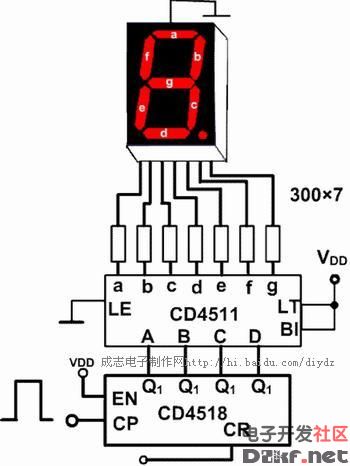
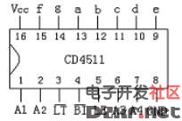
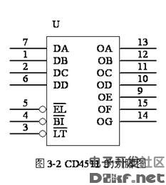
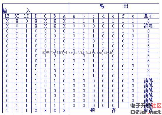
CD4511 is a BCD code for driving common cathode LED (digital tube) display - seven-segment code decoder. Features: CMOS circuit with BCD conversion, blanking and latch control, seven-segment decoding and drive function Larger current draw. Directly drive the LED display. The CD4511 is a CMOS BCD-latch/7-segment decoder/driver with pinouts as shown in Figure 2. Where abcd is the BCD code input and a is the lowest bit. LT is the lamp test terminal. When the high level is applied, the display is normally displayed. When the low level is applied, the display always displays the digital “8â€, and each pen segment is illuminated to check whether the display is faulty. BI is the blanking function end. When the low level is made, all the pen segments are blanked. When the display is normal, the B1 terminal should be added with a high level. In addition, CD4511 has the feature of rejecting pseudo code. When the input data crosses the decimal number 9 (1001), the display glyph also blanks itself. LE is the latch control terminal, latched at a high level, and transmits data at a low level. A ~ g is a 7-segment output that can drive a common cathode LED digital tube. In addition, when CD4511 displays the number "6", the a segment is blanked; when the display number is "9", the d segment is blanked, so when the two numbers 6 and 9 are displayed, the glyph is not very beautiful. Figure 3 is the CD4511 and CD4518. As a one-digit display circuit, if you want to count multiple bits, you only need to cascade the counters, and each stage outputs a CD4511 and LED digital tube. The so-called common cathode LED digital tube means that the cathodes of the 7-segment LED are connected together and should be grounded in the application. The current limiting resistor should be selected according to the power supply voltage. A 300Ω current limiting resistor can be used when the power supply voltage is 5V. The parallel interface between LED and MCU using CD4511 is as follows: CD4511 pin diagram Its function is introduced as follows: BI: The 4 pin is the blanking input control terminal. When BI=0, the seven-segment digital tube is in the extinguished (blanking) state regardless of the state of the other input terminals, and the number is not displayed. LT: The 3 pin is the test input. When BI=1, LT=0, the decoded output is all 1. Regardless of the input DCBA status, the seven segments are illuminated and “8†is displayed. It is mainly used to detect whether the digital tube is damaged. LE: Locks the control terminal. When LE=0, the decode output is allowed. When LE=1, the decoder is in the lock hold state, and the decoder output is held at the value of LE=0. A1, A2, A3, A4 are the 8421BCD code input terminals. a, b, c, d, e, f, g: is the decoding output, the output is high 1 is valid. 1. Pin of CD4511 The CD4511 has a latching, decoding, and blanking function, usually with an inverter as the output stage, which is typically used to drive LEDs. Its pin diagram is shown in Figure 3-2. Name of each pin: where 7, 1, 2, and 6 represent A, B, C, and D, respectively; 5, 4, and 3 represent LE, BI, and LT; 13, 12, 11, 10, 9, 15, and 14, respectively. Represents a, b, c, d, e, f, g, respectively. The left pin indicates the input, the right side indicates the output, and the two pins 8, 16 indicate VDD and VSS, respectively. How does the CD4511 work? 1. The working truth table of CD4511 is shown in Table 3-2. Table 3-2 Truth Table of CD 4511 2. Latch function The latch circuit of the decoder is composed of a transfer gate and an inverter, and the transfer gate is turned on or off by the level state of the control terminal LE. When LE is "0" level on, TG2 is off; when LE is "1" level, TG1 is off, TG2 is on, and there is a latching effect. As shown in Figure 3-3 (3) decoding CD4511 decoding is used by two-level NOR gates. In order to simplify the circuit, first use the two-input NAND gate pair input number. According to the combination of B and C, it is concluded Four items, then the input data A, D together with the NAND gate decoding. (4) blanking BI is the blanking function end. After a certain level is applied to the terminal, the output of the B terminal is forced to be low level, and the glyph is blanked. The blanking control circuit is shown in Figure 3-4. The level of the blanking output J is J= =(C+B)D+BI If you do not consider the blanking BI term, you will get J=(B+C)D According to the above formula, when the BCD code is input from 1010 to -1111, the J terminal is at the "1" level, thereby blanking the glyphs in the display. The corresponding display of the 8421 BCD code is shown in the figure below: Outdoor LED Screen,Advertising Led Display Screen,Outdoor Display Screen,Outdoor Led Advertising Board Shanghai Really Technology Co.,Ltd , https://www.really-led.com


![]()
![]()
