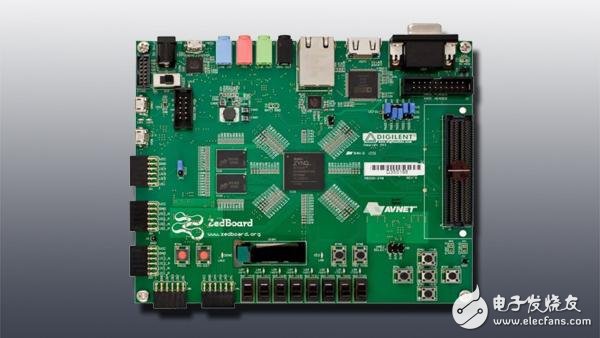
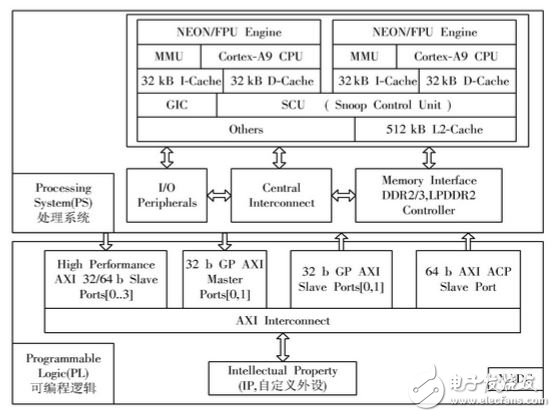
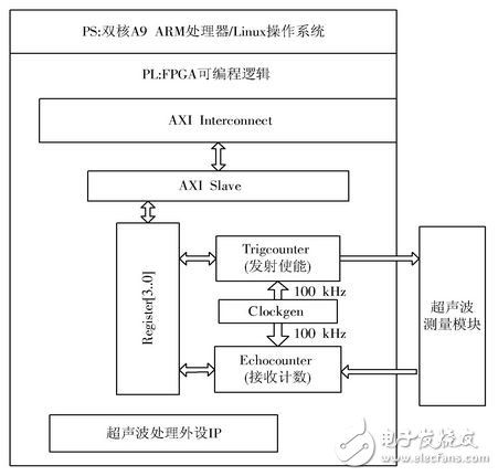
Abstract: In order to accurately measure the obstacle distance, based on the latest Zedboard FPGA (Field Programmable Logic Array) development board, the software and hardware design method of the obstacle distance measurement system is designed. The system provides a complete distance measurement service for the smart car platform, with a range of 2cm~4.5m and an accuracy of 0.2cm. The design includes the entire process from the underlying hardware circuit design, the programmable logic IP (IntellectualProperty) core design, to the Linux device driver design, and has certain reference value for the personnel engaged in the development of software and hardware on the Zynq ⃠7000 FPGA. With the rapid development of integrated circuit manufacturing and application technology, the performance of embedded systems has also been continuously improved, and has been widely used in industrial control, aerospace, military and consumer electronics. Driven by the development of silicon technology and market-driven, Xilinx has introduced a new generation of AllProgrammable Zynq⃠7000 series based on 7 series FPGAs. This series of products integrates the embedded field set-up - dual-core ARM CortexA9 processor and 7 series 28nm process FPGA chip. Zedboard is such an experimental development board based on the Zynqâƒ7000 product, which offers more possibilities for software and hardware design. This article is based on the current state-of-the-art Zedboard FPGA (Field Programmable Logic Array) development board in the FPGA industry. From the underlying hardware circuit design, programmable logic IP (IntellectualProperty) core design, to Linux device driver design, the obstacle distance measurement is realized. The hardware and software system and the distance measurement service are realized on the smart car platform. This method has a guiding role in the development of hardware and software on the Zynqâƒ7000 FPGA. Traditionally, embedded processor cores in FPGAs are based on FPGAs and processors, and the design ideas are based on programmable logic. However, the new generation of fully programmable Zynqâƒ7000 takes a different approach, it is based on the processor, supplemented by FPGA. The FPGA becomes a coprocessor of the ARM processor [1]. Figure 1 is a block diagram of the Zynqâƒ7000 SoC chip. To put it simply, Zynq consists of two parts: PS and PL: PS (Proâƒcessing System) is equivalent to an ARM chip, and PL (Programmable Logic) is equivalent to an FPGA chip. Figure 1: Zynq structure diagram The PS system structure is: dual-core A9 processor, which is the control center of the whole platform. The processing speed is up to 1GHz. It can be enhanced by NEON expansion and single-precision floating-point unit. It has 32KB instruction and data L1 cache, unified 512KBL2 cache and 256KB. On-chip memory; storage interface to manage the storage state of the on-chip system, including DDR3, DDR2 and LPDDR2 dynamic memory controllers and two QSPI, NANDFLASH and NORFLASH controllers; general peripherals, general peripherals in PS are ARM direct Interface for communication with external devices, including SPI, I2C, CAN, UART, GPIO, USB2.0, etc.; other components. The PL part structure is: low-power programmable logic, including 28K~350K logic units, 240K~2180K scalable BlockRAM and 80~900 DSPSlice; XADC, PL built-in 12b analog-to-digital converter; general/custom Peripherals, peripherals in the PL are interfaces between devices in the PL and external communications. When the ARM interface is not enough, you can use the peripheral interface of the PL. The data interaction between the PS and the PL is implemented through the AXI (AdvancedeXtensibleInterface) interface. Specifically: high-performance AXI interface (HighPerformanceAXISlavePorts), a total of four; general AXI interface, including two main device interfaces and two slave device interfaces, a total of four; accelerated coherent port, is a definition of ARM multi-core architecture interface. According to the characteristics of Zynq structure, pay attention to the application system structure design, using a powerful SoC chip such as Zynq, which is different from the general ARM chip and the common FPGA. It requires a collaborative design between hardware and software to achieve the desired performance metrics. In SoC design, IP (IntellectualProperty) technology is an important concept. It is the key to software and hardware co-design. Modules can be reused through standardized IP cores, which can complete large-scale and complex SoCs. Design [3]. This article takes an ultrasonic ranging system as an example to introduce how to customize IP and design Linux device drivers on ZynqSoC, and completely expounds the design process from hardware to software. The system structure of the design is shown in Figure 2. On the PS, run the Linux operating system for the LinaroUbuntu distribution. According to the guidance of the literature [2], the configuration software is completed using Xilinx's development software, so that the PS can run the operating system. Figure 2: System structure diagram The PL part is customized according to the requirements of the system control. The Xilinx AXI bus-based ultrasonic processing peripheral IP core is designed to interact with external ultrasonic transmitting and receiving circuits. Under the Linux operating system, this IP core becomes a device, which requires writing a corresponding device driver to implement the package of the ultrasonic ranging function. We make OBD connector with terminal by ourselves,
soldering type and crimping type are both available. Also 12V and 24V type. OBD1, OB2, J1939, J1708, J1962, etc. Also molded by different
type, straight type or right-angle type. The OBD connector cables used
for Audi, Honda, Toyota, BWM, etc. We have wide range of materials
source , also we can support customers to make a customized one to
replace the original ones. Vehicle Diagnostic Cables,Diagnostic OBD Cable,OBD2 Splitter Y Cables,OBD2 Diagnostic Adapters,OBD Heavy Vehicle Cables ETOP WIREHARNESS LIMITED , https://www.etopwireharness.com

