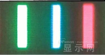
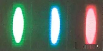
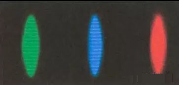
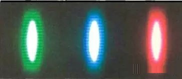
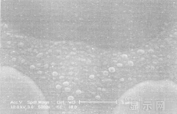
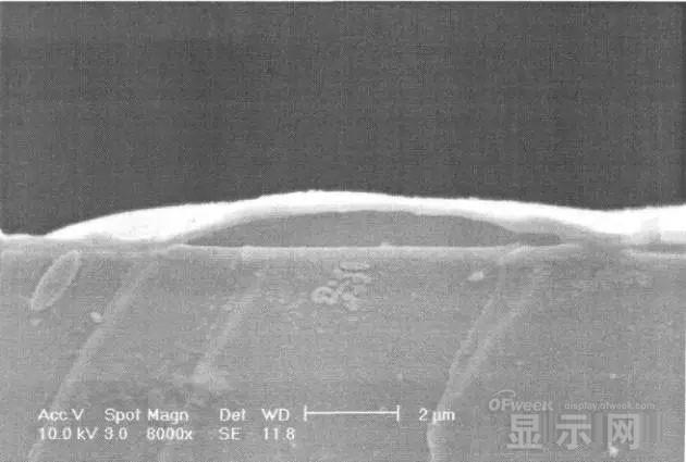
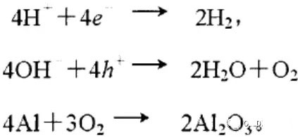
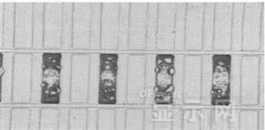
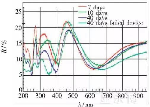
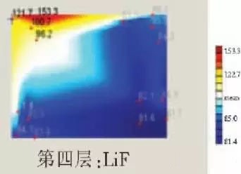
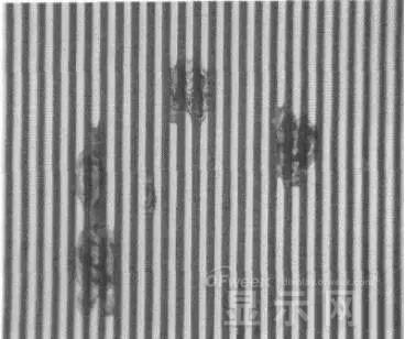
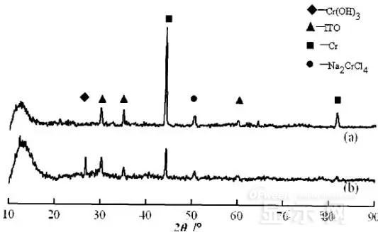
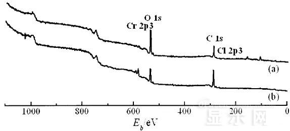
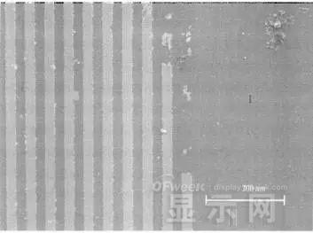
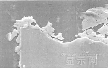
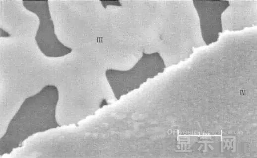
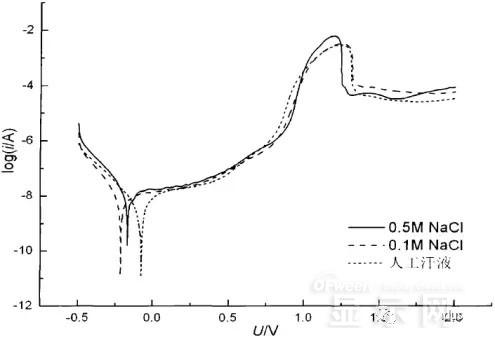
LED semiconductor lighting network news today to see the failure of O LED , OLED failure involves a lot of problems, although the industry has done a lot of research, but the law of failure and the specific mechanism has not been fully revealed. Non-essential degradation factor In general, non-essential degradation is generally classified as long as it is not due to basic properties such as the structure and materials of the components. The most important manifestation of non-essential degradation is the increase in black spots. When the non-illuminated area is gradually increased, the area where the OLED emits light will be relatively reduced, which in turn affects the problem of life. Most of the materials used in OLED devices are extremely sensitive to moisture and oxygen. If the device is not packaged, it is easy to find many black non-light-emitting areas in its light-emitting area, and the black non-light-emitting area will be slower with time. Slower and bigger. The radius of the black region is roughly proportional to the quadratic root of time, which seems to imply that the formation of a black non-illuminated region is associated with a certain diffusion mechanism. Since the black non-light-emitting area is increased to a certain extent, we can see it with the naked eye, so the life of the OLED device is the earliest from the study of black spots. Essential deterioration Although the device can be effectively controlled due to the non-light-emitting region caused by external disturbances, it is found that the luminance of the device is degraded with time even if no black spots are generated. Obviously, this phenomenon is not caused by the outside world. It is the aging of the device, or the decline caused by the material itself. A very clear and perfect theory has not yet been formed to explain the current degradation of OLED devices, which also illustrates the complexity of the inherent degradation factors of OLED devices. Effect of water vapor oxygen on organic materials Many studies have shown that one of the factors affecting the life of organic EL devices is that the presence of water molecules and oxygen plays an important role in the action of organic EL materials, especially water molecules. However, how water molecules and oxygen change the organic layer, many articles at home and abroad have mentioned such problems, such as the oxidation of organic layers, but the specific process is unknown. Luminous area degradation After being sealed for a period of time, the packaged OLED device has a phenomenon that the light-emitting area is reduced or even not illuminated. It has been observed that the adhesive back cover of such a device and the epoxy resin of the glass front cover plated with the device material have voids. This means that the package is not tightly sealed and the air is in direct contact with the device. The reduction in the light-emitting area of ​​the device is likely to be related to such a bonding layer void. Oxygen and water vapor enter the device through the channel, affecting the performance of the device and changing the light-emitting area of ​​the device. The device was shot immediately after opening, because the device was only exposed to air for a few minutes after opening, so it can be seen that the light-emitting area is a relatively complete rectangle, the corners are sharp and angular, the brightness is uniform, and the three colors of red, green and blue alternate. After 30 minutes of power-on, the visible light-emitting area has been blurred from the four corners. The longer the time, the greater the change. The reduction in device area begins at the four corners of the device. This is because oxygen vapor intrudes into the interior of the device primarily through the edge of the device. Wet nitrogen environment The experiment ruled out the effects of oxygen and examined the effects of water vapor on the device. Obtain a humid nitrogen environment by: 1. Place the unsealed device in the system. 2. After connecting the wires, seal the other parts than the catheter 3. Completely close the system after continuous nitrogen flow for a period of time. 4, power on observation photo Failure device morphology analysis Observation of the device after failure revealed that the cathodes of the three color devices had different degrees of bubble-like protrusion structures. The color of the cathode at the edges and corners changes, and bubbles are randomly distributed inside the device. The area where the color of the cathode changes changes to a non-light-emitting area, and the bubble still emits light. In the SEM micrograph, it can be clearly seen that the cathode has different sizes of protrusions. A cross-sectional view of the bulge. Phenomenon analysis The reason why the color of the cathode changes is mainly because oxygen enters the inside of the device from the edge and acts on the cathode to oxidize the cathode to generate a non-light-emitting region. The reason for the bubble on the cathode is that some tiny dust particles are deposited on the organic layer before the cathode to form pinholes, and because water vapor is easily adsorbed on the surface of the device, it enters through the pinholes on the surface of the Al electrode. Inside the device, it is decomposed by the action of current, and the decomposed gas will generate a certain pressure to the AI ​​electrode due to the high temperature expansion, so that the Al electrode and the organic layer are separated, thereby generating bubbles. The gas lifts the cathode up to form a voided raised structure. The cathode is separated from the organic layer, and electron injection is affected, resulting in a non-luminous region on the device. The effect of water on the degradation of the luminescence area of ​​the device is more pronounced and faster than that of oxygen. Under the combined action of water and oxygen, the device will quickly fail. Therefore, the hermeticity of the device package is very important for the stability of the O LED . Bubble area beyond the edge of the device The interface between the organic material and the metal electrode is very uneven. When the device works, a non-uniform electric field is formed, causing the current to be too large at some points, and the short circuit becomes a "hot spot", and the oxidized metal electrode causes failure and forms a black spot. At the same time, local overheating causes the organic material to melt, and the raised bubbles provide space for the flow of the molten organic material, so the situation shown in the above figure appears, and the overflow of the organic material is observed, and the bubble area on the device exceeds the edge of the device. . Water vapor and oxygen have a large effect on the rate of device area degradation. In the presence of moisture, energization can cause water to decompose to produce gas that pushes up the cathode metal layer while providing room for molten organic matter flow due to local overheating. In the unenergized area, crystallization of organic matter may occur, which may also affect the luminescence properties of the device. Oxygen oxidizes the cathode material and the organic layer, resulting in the generation of non-luminescent regions. OLED device structure analysis OLED is a multilayer organic thin film device, which makes the structure of OLED almost impossible to analyze by traditional characterization methods, and the difference in film thickness of each layer has an important influence on the performance of OLED. The sample was subjected to room temperature aging for 7, 10, 40 days using a film analyzer to obtain a reflectance curve of the sample, as shown in the following figure. To speed up device failure, a point of aging of the 40-day device is disabled to disable it, and the reflectance at this point of failure is tested and compared to the reflectance profile of the non-failed device. The intact samples and the failed samples aged for 40 days were selected for further thickness comparison tests. The thickness test of the sample that failed after electrification after 40 days of aging is shown in the figure. The table below is a comparison of the thickness averages (the failure point is 12 good points with the other parts). In order to reduce the amount of calculation, the thickness of the ITO layer and the NPB layer were fixed after repeated tests, and only the thicknesses of the other two layers were calculated and fitted. Comparison of the average of the failure point and the thickness of the intact point Electrode lead corrosion The electrode lead is a portion that connects the voltage to drive the electrode of the light emitting device, and the corrosion directly destroys the electrical connection between the driving and the O LED device, resulting in device failure. Therefore, it is important to find out the mechanism of electrode lead corrosion and propose a control scheme to reduce the occurrence of such phenomena. Device display defect Corrosion electrode microscopic morphology leading to this phenomenon OLED lead ITO is widely used in optoelectronic devices due to its transparency to visible and near-infrared light, and OLEDs use ITO as a transparent anode. The lead and the anode are simultaneously made of ITO, so that the pattern can be formed by one photolithography process. Since the ITO alone is not sufficiently low in lead resistance, the Cr metal plating can improve the lead conductivity. At the same time, Cr can form a dense surface oxide layer in air or in an oxidizing acid atmosphere at room temperature, has corrosion resistance to many chemical media, and has excellent corrosion resistance in various environments, so it can also be used as a lead protection. Floor. experiment analysis In order to analyze the cause of lead corrosion, the polarization material was measured and analyzed. The electrode lead material was cut into small pieces of 10 mm × 8 mm, washed and dried, and the wires were wound on one side, and the wires were wrapped with a paraffin rosin mixture to prevent the wires from being exposed. A surface of the lead material of about 6 mm × 8 mm was left as a working surface. The test medium is 0.5mol/L, 0.1mol/L NaCl solution and artificial sweat solution (deionized aerated aqueous solution containing 0.5% sodium chloride, 0.1% lactic acid, 0.1% urea) The temperature is controlled at 25 °C. The experiment found that when the lead sample just corroded, a brown liquid was formed on the surface of the sample, and the water evaporated to form a solid corrosion product, which remained on the surface of the sample. To analyze the corrosion product composition, an XRD test was first performed, and the samples were an unetched lead sample (a) and a corrosion lead sample (b), respectively. XRD pattern of uncorroded lead sample (a) and corrosion lead sample (b) Sample (b) showed a diffraction peak of Cr(OH)3 hydrate at 26.77°, while this peak did not appear in sample (a); at the same time, metal Cr in sample (b) was at 44.30° and The diffraction kurtosis of 81.72° is significantly weakened; this indicates that during the etching process, the metal Cr in the lead sample reacts to form Cr(OH)3. XPS spectra of unetched lead sample (a) and corroded lead sample (b) The binding energy of Cls was 285 ev, and the binding energy peak of Cr in sample (a) was 577.4 ev, corresponding to Cr2O3, where Cr was positive trivalent; the binding energy of Cr in sample (b) was 579. 6ev, corresponding to CrO3, where Cr is a positive hexavalent. It can be seen that positive hexavalent Cr is generated during the corrosion process. In addition, XPS results show the presence of Cl, and the ion concentration is 0.1% or more. Sample morphology 60 times 2000 times The SEM analysis of the corrosion lead samples was carried out, and it was found that the samples were clearly divided into three steps. The region I is a portion where Cr and ITO are completely etched away in the photolithography process; the region II is a region where the lead is completely etched; the region III is an incompletely etched region; and the region IV is an unetched region. EDX measurement In order to distinguish the composition of each step, the EDX spectrum analyzes the elements of different parts of the corrosion sample to determine the structure of the corrosion sample. EDX results from different areas of the corroded lead sample The region II where the lead is completely corroded has no Cr and In elements present, and is identical to the region I; the energy spectrum of the region III shows that there is no Cr element and the In element exists; the region IV is an uncorroded region, and the energy spectrum results show the Cr and In elements. Both exist. From this it can be determined that the occurrence of corrosion is from top to bottom: the surface layer of Cr first corrodes, then ITO. Polarization curve analysis Polarization curves of leads in different solutions In the first half of the curve, the properties of the Cr coating are reflected. In the reaction, Cr gradually dissolves, and the latter part of the curve shows the properties of the ITO exposed after the Cr layer is dissolved. Cr shows better passivation characteristics in the experimental medium. However, as the electrode position increases, the current density increases gradually, and the dissolution rate of Cr increases. In the latter half of the curve, the current density in the 0.5M NaCl solution is relatively high, while the current density of the 0.1M NaCI solution and the artificial sweat solution (the chloride ion concentration is about 0.086 M) with relatively low chloride ion concentration. It is much lower. It can be seen that chloride ions promote the corrosion of ITO. During the corrosion process, the Cr coating reacts to form Cr(OH)3 and CrO3, which is caused by the difference in the potential of Cr during the reaction: at a lower potential, Cr dissolves in a trivalent form; at a higher potential, Cr Passivation dissolution occurred and dissolved in hexavalent form. After the Cr plating layer is dissolved, the ITO is subsequently corroded. Among them, chloride ion promotes the corrosion of ITO: the higher the chloride ion concentration, the faster the ITO corrosion rate. In view of the above findings, it is recommended to take the following measures to control the occurrence of electrode lead corrosion: 1. Residual chloride ions in the photolithography process cause damage to the passivation film of Cr and accelerate the corrosion of ITO. It is recommended to optimize the cleaning process to reduce the residual content. 2, to prevent the occurrence of electrode lead corrosion, the key is to control the corrosion of the Cr coating. It is recommended to apply a protective film to the electrode part to prevent the electrochemical reaction between Cr and the adsorbed liquid. CT For Three-phase Electricity Meters
Our company`s current transformers have high precision,wide range,small volume and good linearity that can be used to the field of electronic watt-hour meter, electric energy metering, electronic detection.
Performance
â—Power frequency insulation strength:The insulation between the primary winding and the secondary winding and the ground part of the CT can bear 4kV power frequency voltage for 1minute
â—Interturn insulation strength:The secondary open circuit, the primary winding through the rated current 1min, no inter-turn damage in the transformer
â—The deviation is better than the industry standards and national standards
Three-Phase Electricity Meters Ct,Dc Resistance Current Transformer,Best Ct For Dc Resistance,New Design Ct Anyang Kayo Amorphous Technology Co.,Ltd. , https://www.kayoamotech.com