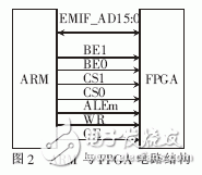
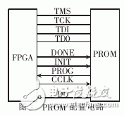
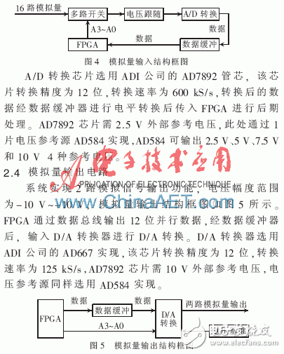
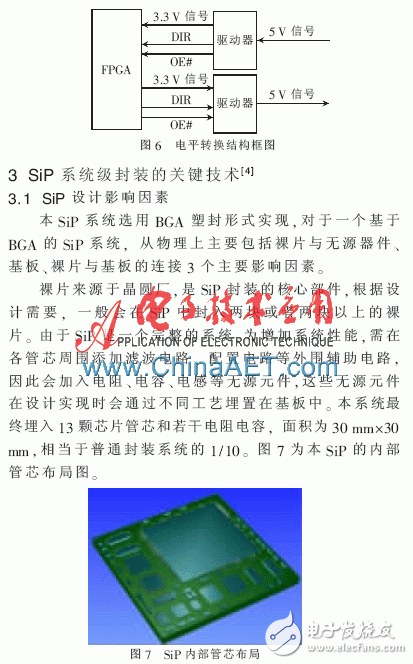
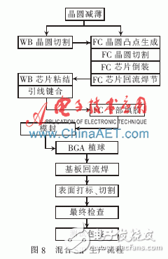
Abstract: This paper introduces the concept and characteristics of system-level packaging, and expounds the key technologies and basic production realization processes of SiP design. A SiP general-purpose microprocessor system based on ARM and FPGA dies is designed. The overall block diagram of the SiP system is introduced, and the functional structure of each part of the system is analyzed in detail. The system has the advantages of small size, low power consumption and complete functions, which fully demonstrates the superiority of SiP technology. Packaging is a bridge connecting semiconductor chips and electronic systems. With the rapid development of the semiconductor industry and its rapid penetration into various industries, electronic packaging has gradually become a key technology for realizing the functions of semiconductor chips, and has been increasingly attention. In recent years, the urgent need for embedded system design in consumer electronics and special application environments has driven the rapid development of the electronic packaging industry. Electronic packaging technology is moving toward multi-functionality, high integration, high reliability, miniaturization, etc., and applications have expanded from the traditional consumer electronics field to radar, sonar, medical imaging and petroleum exploration. At present, the industry's highly integrated electronic systems mainly include system-on-chip (SoC) and system-in-package (SiP). SoC technology is relatively mature and has been widely used in electronic systems, but it is increasingly limited by process and reliability. SiP is a new SoC-based packaging technology that stacks high-performance modules of one or more chips and passive components in a single die in a single die, thereby upgrading the package from a single chip to a system level. Chip [1]. Compared with SoC, SiP has the advantages of low system development cost, short development cycle, high integration and high reliability. The features of SiP technology can be customized, small size, low power consumption and light weight to adapt to the development needs of embedded systems, and more and more attention and application in the embedded field. This paper designs a SiP system-level package using ARM and FPGA die design. The system encapsulates a multi-function general-purpose microprocessor system in a small SiP chip, which is small in size, low in power consumption and functional. Complete, to achieve a high degree of integration of the system. Figure 1 is a block diagram of the internal structure of SiP. The SiP system-level package is built with ARM processor and FPGA controller as the core. ARM is the main processor, responsible for the control and management of the whole system; FPGA as the main bridge controller of the system, complete the comprehensive scheduling management of the system multi-function peripherals. FPGA internally completes control logic such as discrete, PWM, serial, A/D, D/A, and realizes 16 analog inputs, 2 analog outputs, 8 PWM inputs, 16 PWM outputs, and 5 discrete inputs. 5 channels of discrete output, 6 channels of RS-232, 6 channels of RS-422, 1 channel of RS-485 and other functions. Unlike traditional packaged devices, all devices selected for SiP system-level package design are chip dies. In this system design, ARM Labs uses SIM3U167 ARM Cortex-M3 die from Silicon Labs, and FPGA selects XQV6000 from Xilinx. The die, other functional circuits of the system (such as PROM circuit, A/D and D/A circuit, interface drive circuit) are all designed with corresponding chip die. The final implementation form of the SiP system is a BGA304 plastic package chip. All function signals, CPU downloads, FPGA downloads, and power signals are all pinned to the chip pins. In the design, the chip also reserves some general-purpose I/O pins to realize the custom functions during user development. By building a simple basic peripheral circuit, users can implement a complete and complex system with the above functions. As the CPU of the system, ARM is responsible for the control and management of the whole system. Figure 2 shows the connection structure between ARM and FPGA circuits [2]. Among them, EMIF is an external memory bus. The ARM chip supports two modes of address data division mode and multiplexing mode. In the multiplexing mode, up to 24 bits of data can be supported. The system selects the multiplexing mode, and EMIF_AD15:0 is 16 Bit address data multiplex bus. ARM controls the FPGA chip through the WR write enable signal, OE read enable signal, ALEM address latch signal, CSx chip select signal and BEx byte enable signal to control the peripheral circuits of the system. Among them, the ALEm signal and the BEx signal are only used in the multiplexing mode. The SIM3U167 chip used in the system is a high-performance processor with 256 KB Flash and 32 KB SRAM on-chip memory, supporting many peripheral common interfaces. According to the design requirements, this system introduces 1 UART, 1 USART, 1 SPI, 1 I2C, 1 USB, 2 12-bit A/D conversion, 2 10-bit D/A conversion interface signals to SiP. On the external pin. FPGA generally needs PROM chip to store logic loading file. This system selects SM18V04 die of Guowei Company as the peripheral configuration device of FPGA. The die is divided into parallel loading and serial loading [3]. Here, the serial loading mode is selected. In this mode, the data is loaded with configuration data at a rate of one bit per TCK, and the loading speed can reach 33 MHz. The structure of the PROM configuration circuit is shown in Figure 3. In addition to TDI, TDO, TMS, and TMK four JTAG-specific Boundary-Scan signals, a set of control signals is required between the FPGA and the PROM, including D0 (Configuration Data Input), CCLK (Configuration Clock), DONE (FPGA Configuration Complete), PROG (trigger reconfiguration) and INIT (configuration initialization) 5 signals. When power-on, PROM loads the configuration data into the FPGA through these control signals to start the system running normally. The system has 16 analog signal acquisition functions, the voltage range is -10 V~+10 V, and the block diagram is shown in Figure 4. The signal is strobed by one 16-select 1 multiplexer to modulate one of the 16 analog signals for A/D conversion, and the FPGA generates channel selection signals A3~A0 to determine which analog signal to finally convert. The multiplexer is implemented by the ADG506 die of Analog Devices. The signal strobed by the multiplexer is subjected to voltage follow-up processing by a first-stage operational amplifier. The input impedance of the voltage follower is very large, and the output impedance is very small, which can increase the load on the channel. ability. The external discrete and PWM input signals are both 5 V TTL level, and the signal that the FPGA can process is 3.3 V CMOS level. Therefore, the discrete and PWM signals need to be level-converted by the driver during input and output. The conversion structure is shown in Figure 6. The driver uses the SM164245 die of Guowei Company. The chip consists of two sets of 8-bit bidirectional data buffers. Each set of data buffers is controlled by a DIR direction control signal and an OE# enable signal. Both signals are generated by FPGA logic. The final processing of PWM and discrete quantities is also implemented by FPGA logic. The substrate [5] selects factors such as the thermal expansion coefficient CTE, dielectric constant, dielectric loss, electrical resistivity and thermal conductivity of the general reference material. Commercial SiP products generally choose organic substrates, which are based on high-density multilayer wiring and micro-hole substrate technology. They have low interconnect resistance and dielectric constant, and low cost, but there is CTE between chip and substrate. Limitations such as high difference, large thermal mismatch, and poor stability. Industrial grade products generally use high-cost ceramic substrates, which have excellent heat dissipation, good air tightness and high reliability. The die and the substrate are usually connected by wire bonding and Flip-Chip. Wire Bonding is flexible, low cost, and highly reliable, but with low connection efficiency and low welding accuracy. Flip-Chip has the advantages of strong solder joints, short signal transmission path, wide power/ground distribution, high I/O density, small package size and high reliability, but the processing cost is relatively high. SiP is generally in BGA plastic package or ceramic package [3], so the processing and production process is mainly the Wire Bonding BGA (WB-BGA) and FlipChip BGA (FC-BGA) processes commonly used in BGA packages. However, since the SiP system-level package is formed by stacking multiple dies, it is not exactly the same as the ordinary single-function BGA chip. It may be encountered that both the WB process chip and the FC process chip are supported in the die. At this point, a mixed SiP process flow is required. Figure 8 shows the flow chart of the SiP mixing process flow. Compared with the general SiP package design, the system has many types and large numbers of buried dies and passive components, and finally is realized by a mixed process. This paper introduces the key technology and production realization of SiP design, and based on this, elaborates a SiP system-level packaging system realized by ARM and FPGA. The chip has complete functions and stable performance, compared with the traditional single. The board system has the advantages of being customizable, small in size, low in power consumption, light in weight, etc., and is worthy of being popularized in the future micro processing system. SiP technology is a rapidly developing IC packaging technology, which is receiving more and more attention and promotion. It will become the mainstream development direction of future electronic packaging and provide a new solution for the development of embedded systems.
UCOAX Custom Made various Adapters to easy connect different interfaces.
Lightweight and Portable/Efficient and Time-Saving/Universally Compatible Adapters design make life and work easier.
The reversibility of USB-C Connector
enables you to plug it without checking the orientation, which saves plentiful
time and improves efficiency.
Usb C Adapter,Usb Adapter,Power Adapter,Type C Adapter, USB-C TO USB Female Adapter UCOAX , https://www.ucoax.com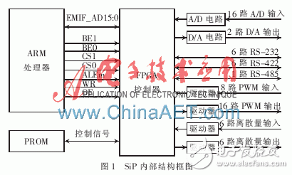
Package design of SiP universal microprocessor system based on ARM and FPGA
Such USB-C Port and USB-A Port, Power Adapter Means No extra Cable needed.