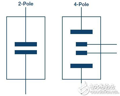
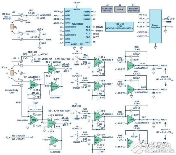
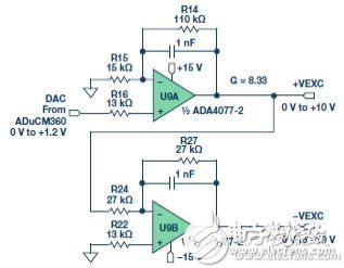
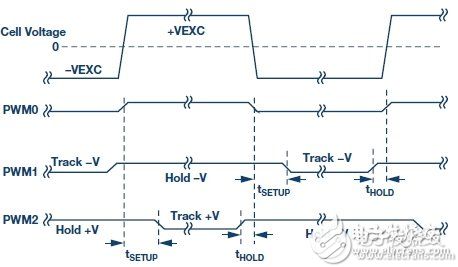
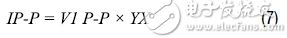
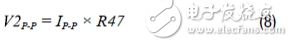
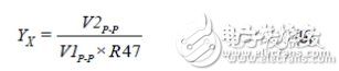
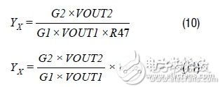
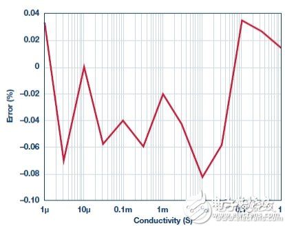
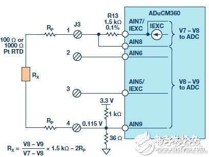
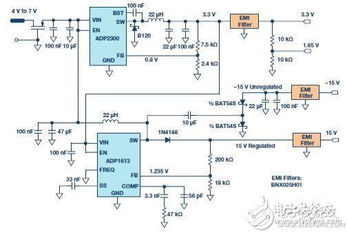
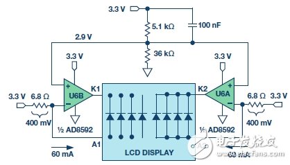
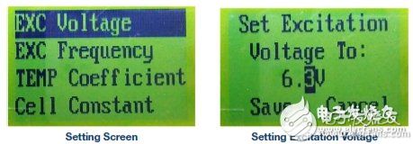
As water quality monitoring becomes more important, a variety of related sensors and signal conditioning circuits have been developed. Water quality measurements include bacterial count, pH, chemical composition, turbidity and conductivity . All aqueous solutions are electrically conductive to some extent. Adding an electrolyte such as a salt, an acid or a base to pure water can increase the electrical conductivity and lower the electrical resistivity. This article focuses on conductivity measurements. Pure water does not contain a large amount of electrolyte, and when the sample is at a certain voltage, it can only conduct a small current - so its conductivity is very low. Conversely, if there is a large amount of electrolyte in the sample, more current will be conducted - its conductivity is higher. We look at the conductivity more from the perspective of resistance rather than conductance, but the two are reciprocal. The resistivity Ï of a material or liquid is defined as the electrical resistance of the material when it is in fully conductive contact with the opposite side of the cube-shaped material. The resistance R of other shaped materials can be calculated as follows: R = Ï L /A (1) among them: L is the contact surface spacing. A is the contact area. The resistivity is measured in ? cm. When touching 1 cm &TImes; 1 cm &TImes; 1 cm cube facing opposite, the resistance of the 1 cm material is 1 Ω. Conductance is the reciprocal of the resistance and conductivity is the reciprocal of the resistivity. The unit of measurement for conductance is Siemens (S), and the unit of measurement for conductivity is S/cm, mS/cm or μS/cm. In this context, Y is a general symbol of conductivity, measured in S/cm, mS/cm or μS/cm. However, in many cases, for convenience, we will omit the distance term and the conductivity is only expressed as S, mS or μS. Measuring conductivity using a conductivity cell The conductivity measurement circuit measures conductivity by connecting to a Sensor immersed in a solution (called a conductivity cell), as shown in Figure 1. Figure 1. Connection of Conductivity Cell to Conductivity Measurement Circuit (EVAL-CN0359-EB1Z) The measuring circuit applies an alternating voltage to the sensor and measures the amount of current generated, which is related to the conductivity. Since the conductivity has a large temperature coefficient (up to 4%/°C), the circuit incorporates the necessary temperature sensor to adjust the reading to a standard temperature, typically 25°C (77°F). When measuring a solution, the temperature coefficient of the conductivity of the water itself must be considered. In order to accurately compensate for the temperature, an additional temperature sensor and compensation network must be used. Contact sensors typically include two electrodes that are insulated from each other. The electrodes are typically Type 316 stainless steel, titanium palladium alloy or graphite with specific sizes and spacing to provide known electrode constants. Theoretically, a 1.0/cm electrode constant represents two electrodes, each having an area of ​​1 cm2 and a pitch of 1 cm. For a specific operating range, the cell constant must match the measurement system . For example, if a sensor having a cell constant of 1.0/cm is used in pure water having a conductivity of 1 μS/cm, the resistance of the conductivity cell is 1 MΩ. In contrast, the same conductivity cell has a resistance of 30 Ω in seawater. Due to the large range of resistance changes, it is difficult for ordinary instruments to accurately measure such extreme conditions with a single electrode constant. When measuring 1 μS/cm solution, the conductivity cell is equipped with large-area electrodes with small electrode spacing. For example, for a conductivity cell with a cell constant of 0.01/cm, the conductivity of the cell is measured to be approximately 10 kΩ instead of 1 MΩ. Accurate measurement of 10 kΩ is easier than measuring 1 M? Therefore, for ultrapure water and high conductivity seawater, using conductivity cells with different cell constants, the meter can operate within the same cell resistance range. The electrode constant K is defined as the ratio of the distance L between the electrodes to the area A of the electrode: K = L/A (2) Then, the instrument measures the conductance of the conductivity cell Y: Y = I/V (3) The liquid conductivity YX can be calculated as follows: YX = K × Y (4) There are two types of conductivity cells: one with two electrodes and the other with four electrodes, as shown in Figure 2. The electrodes are often referred to as poles. Figure 2. Bipolar and quadrupole conductance cells. Bipolar sensors are more suitable for low conductivity measurements, such as pure water and various biological and medical liquid quadrupole sensors, which are more suitable for high conductivity measurements such as wastewater and seawater analysis. The electrode constant of the bipolar conductivity cell ranges from approximately 0.1/cm to 1/cm, while the electrode constant of the quadrupole conductance cell ranges from 1/cm to 10/cm. The quadrupole conductance cell eliminates errors caused by electrode polarization and electric field effects; these errors can interfere with the measurement. The actual configuration of the electrodes can be parallel rings, coaxial conductors, etc., rather than a simple parallel plate as shown in FIG. Regardless of the type of cell, no DC voltage can be applied to the electrodes because ions in the liquid can collect on the electrode surface, causing polarization effects and measurement errors, and are more likely to damage the electrodes. If a coaxial sensor is used, attention should be paid to the shielding of the sensor. The shield electrode must be connected to the same potential as the metal container holding the liquid. If the container is grounded, the shield electrode must be connected to the ground of the board. In addition, it is necessary to ensure that the excitation signal does not exceed the rating of the excitation or excitation current of the cell. The circuit allows programmable excitation voltages ranging from 100 mV to 10 V, and the R23 (1 kΩ) series resistor limits the maximum cell current to 10 mA. Circuit description The circuit in Figure 3 is a fully independent, microprocessor-controlled, high-precision conductivity measurement system for measuring liquid ion content, water quality analysis, industrial quality control, and chemical analysis. The carefully selected combination of precision signal conditioning components provides better than 0.3% accuracy over a 0.1 μS to 10 S (10 M? to 0.1 Ω) conductivity range without calibration. Automatic detection for 100? or 1000? platinum (Pt) resistance temperature sensors (RTD) allows conductivity to be measured with room temperature as a reference. The system supports two-wire or four-wire conductivity cells as well as two-wire, three-wire or four-wire RTDs for increased accuracy and flexibility. The circuit produces a precise AC excitation voltage with minimal DC offset, thereby avoiding damage to the polarization voltage on the conductivity electrode. The user can programmatically control the amplitude and frequency of the AC excitation signal. Innovative simultaneous sampling technology converts the peak-to-peak amplitude of the excitation voltage and current into a DC value, which not only improves accuracy, but also simplifies the processing of signals by a dual 24-bit Σ-Δ ADC built into a precision analog microcontroller. . An intuitive user interface is achieved with LCD displays and encoder buttons. The circuit can communicate with a PC using the RS-485 interface as needed, and operates from a single 4 V to 7 V supply. The excitation square wave of the conductivity cell is generated by switching the ADG1419 between the +VEXC and −VEXC voltages using the PWM output of the ADuCM360 microcontroller. The square wave must have a precise 50% duty cycle and a very low dc offset voltage. Even a small dc offset voltage can damage the conductivity cell after a period of time. Figure 3. High-performance conductivity measurement system (schematic diagram: all connections and decoupling are not shown). The +VEXC and −VEXC voltages are generated by the ADA4077-2 op amps (U9A and U9B). The magnitude of these two voltages is controlled by the DAC output of the ADuCM360, as shown in Figure 4. Figure 4. Excitation voltage source. The ADA4077-2's offset voltage is typically 15 μV (Class A) with a bias current of 0.4 nA, an offset current of 0.1 nA, an output current of up to ±10 mA, and a dropout voltage of less than 1.2 V. The U9A op amp has a closed-loop gain of 8.33 that converts the ADuCM360's internal DAC output (0 V to 1.2 V) to a +VEXC voltage from 0 V to 10 V. The U9B op amp reverses +VEXC to produce the −VEXC voltage. Select R22 so that R22 = R24||R27 to eliminate the first-order bias current. The error due to the U9A's 15 μV offset voltage is approximately (2 × 15 μV) ÷ 10 V = 3 ppm. Therefore, the main error produced by the inverting stage is the resistance matching error between R24 and R27. The ADG1419 is a 2.1 Ω on-resistance single-pole, double-throw analog switch with an on-resistance flatness of 50 mΩ in the ±10 V range, making it ideal for generating symmetrical square-wave signals from ±EXC voltages. The symmetry error caused by ADG1419 is usually 50 m? ÷1 k? = 50 ppm. Resistor R23 limits the maximum current through the sensor to 10 V / 1 k? = 10 mA. The voltage V1 applied to the conductivity cell is measured using the AD8253 instrumentation amplifier (U15). The U15 positive input is buffered by the ADA4000-1 (U14). The ADA4000-1 was chosen because it has a low bias current of 5 pA to minimize the low current measurement error associated with low conductivity. The negative input of the AD8253 does not require buffering. The synchronous sampling stage eliminates the offset voltage of U14 and U15, so that measurement accuracy is not affected. The U15 and U18 use the AD8253 10 MHz, 20 V/μs, programmable gain (G = 1, 10, 100, 1000) instrumentation amplifier with a gain error of less than 0.04%. The AD8253 has a slew rate of 20 V/μs and a 0.001% settling time of 1.8 μs (G = 1000). Its common mode rejection is typically 120 dB. The U19 (ADA4627-1) stage is a precision current-to-voltage converter that converts the current flowing through the sensor into a voltage. The ADA4627-1 has an offset voltage of 120 μV (typ., Class A), a bias current of 1 pA (typ), a slew rate of 40 V/μs, and a 0.01% settling time of 550 ns. The device's low bias current and low offset voltage make it an ideal choice for this stage. The 120 μV offset error produces a symmetry error of only 120 μV/10 V = 12 ppm. The U22A and U22B (AD8542) buffers provide a 1.65 V reference for the U18 and U15 instrumentation amplifiers, respectively. The remaining devices on the voltage channel signal path (U17A, U17B, U10, U13, U12A, and U12B) are described below. The current channels (U17C, U17D, U16, U21, U20A, and U20B) work the same. The ADuCM360 can generate PWM0 square wave switching signals for use with the ADG1419 switch, and can also generate PWM1 and PWM2 synchronization signals for simultaneous sampling stages. The voltage of the conductivity cell and the three timing waveforms are shown in Figure 5. Figure 5. Cell voltage and sample-and-hold timing signals. The AD8253 instrumentation amplifier (U15) output drives two parallel sample-and-hold circuits; these two circuits consist of the ADG1211 switch (U17A/U17B), series resistor (R34/R36), holding capacitor (C50/C73), and unity-gain buffer ( U10/U13) composition. The ADG1211 is a low charge injection, quad single-pole, single-throw analog switch with an operating supply voltage of ±15 V and an input signal of up to ±10 V. The maximum charge injection caused by the switch is 4 pC, resulting in a voltage error of only 4 pC ÷ 4.7 μF = 0.9 μV. The PWM1 signal allows the U10 sample-and-hold buffer to be sampled during the negative period of the sensor voltage and then held until the next sample period. Therefore, the U10 sample-and-hold buffer output is equal to the DC level corresponding to the sensor voltage square wave negative amplitude. Similarly, the PWM2 signal causes the U13 sample-and-hold buffer to be sampled during the positive period of the sensor voltage and then held until the next sample period. Therefore, the U13 sample-and-hold buffer output is equal to the DC level corresponding to the positive amplitude of the sensor voltage square wave. The sample-and-hold buffer (ADA4638-1) has a typical bias current of 45 pA, while the ADG1211 switch has a typical leakage current of 20 pA. Therefore, the worst case leakage current of the 4.7 μF holding capacitor is 65 pA. For a 100 Hz excitation frequency, the period is 10 ms. Half cycle due to 65 pA leakage current ( 5 ms) The internal voltage drop is (65 pA × 5 ms) ÷ 4.7 μF = 0.07 μV. The offset voltage of the ADA4638-1 zero-drift amplifier is typically only 0.5 μV, and its error contribution is negligible. The final stage on the signal chain in front of the ADC is the ADA4528-2 inverting attenuators (U12A and U12B) with a gain of −0.16 and a common-mode output voltage of +1.65 V. The offset voltage of the ADA4528-2 is typically 0.3 μV, so the error contribution is negligible. The attenuator stage reduces the ±10 V maximum signal to ±1.6 V and a common-mode voltage of 1.65 V. This range is comparable to the input range of the ADuCM360 ADC, which is 0 V to 3.3 V (1.65 V ± 1.65 V) with a 3.3 V AVDD supply. The attenuator stage also provides noise filtering with a −3 dB frequency of approximately 198 kHz. The differential output of voltage channel VOUT1 is applied to the AIN2 and AIN3 inputs of the ADuCM360. The differential output of current channel VOUT2 is applied to the AIN0 and AIN1 inputs of the ADuCM360. The two equations for calculating the output are as follows: The conductivity cell current is determined by: The V2P-P voltage is determined by: Solve the IP-P of Equation 8, and then substitute Equation 7 to find YX: Solving V1P-P and V2P-P of Equations 5 and 6, and then substituting Equation 9, finds: Equation 11 shows that the conductivity measurement depends on G1, G2, and R47, and the ratio of VOUT2 and VOUT1. Therefore, the ADuCM360's built-in ADC eliminates the need for a precision voltage reference. The AD8253 gain error (G1 and G2) has a maximum value of 0.04%, and R47 selects a 0.1% tolerance resistor. From this point on, the resistance of the VOUT1 and VOUT2 signal chains determines the overall system accuracy. The software's gain for each AD8253 is set as follows: • If the ADC code exceeds 94% of full scale, the gain of the AD8253 is reduced by a factor of 10 in the next sample. • If the ADC code is below 8.8% of full scale, the gain of the AD8253 is increased by a factor of 10 in the next sample. System accuracy measurement The following four resistors affect the accuracy of the VOUT1 voltage channel: R19, R20, R29, and R31. The following five resistors affect the accuracy of the VOUT2 current channel: R47, R37, R38, R48, and R52. Assuming all 9 resistors are 0.1% tolerance and include the 0.04% gain error of the AD8253, the worst-case error analysis indicates an error of approximately 0.6%. The analysis is in the CN-0359 Design Support Package. In practical applications, the resistance error is more likely to be combined by the RSS method, and the RSS error caused by the resistor tolerance on the positive or negative signal chain is √5 × 0.1% = 0.22%. Accuracy measurements were made using 1 Ω to 1 MΩ (1 S to 1 μS) precision resistors to simulate the conductivity cell. Figure 6 shows the results with a maximum error of less than 0.1%. Figure 6. Systematic error (%) versus conductivity (1 μS to 1 S). RTD measurement The accuracy of the conductivity measurement system can only be optimized with temperature compensation. Since common solution temperature coefficients vary between 1%/°C and 3%/°C or higher, measuring instruments with adjustable temperature compensation must be used. The temperature coefficient of the solution is somewhat non-linear and usually varies with the actual conductivity. Therefore, calibration at the actual measurement temperature can achieve the best accuracy. The ADuCM360 has two matching software configurable excitation current sources. They are individually configurable and offer a 10 μA to 1 mA current output with a match better than 0.5%. The current source allows the ADuCM360 to easily perform two-wire, three-wire or four-wire measurements for the Pt100 or Pt1000 RTD. The software also automatically detects if the RTD is Pt100 or Pt1000. A simplified schematic of how different RTD configurations work is given below. All mode switching is done in software without changing the external jumper settings. Figure 7 shows a four-wire RTD configuration. Figure 7.4 Line RTD connection configuration. The pin parasitic resistance of each connected remote RTD is expressed in RP. The excitation current (IEXC) flows through a 1.5 kΩ precision resistor and RTD. The on-chip ADC measures the voltage across the RTD (V6 – V5) and uses the voltage across R13 (V7 – V8) as the reference voltage. It is important to select the R13 resistor and the IEXC excitation current value so that the maximum input voltage of the ADuCM360 on AIN7 does not exceed AVDD − 1.1 V; otherwise, the IEXC current source will operate abnormally. The RTD voltage can be accurately measured using two sense pins connected to AIN6 and AIN5. The input impedance is approximately 2 MΩ (no buffer mode, PGA gain = 1), and the error caused by the current flowing through the sense pin resistance is minimal. The ADC then measures the RTD voltage (V6 − V5). The RTD resistance can then be calculated as follows: The measured value is a proportional value and is independent of the exact external reference voltage and is only related to the 1.5 kΩ resistor tolerance. In addition, the four-wire configuration eliminates pin-related errors. The ADuCM360 offers input options with and without buffering. If the internal buffer is activated, the input voltage must be greater than 100 mV. The 1 kΩ/36 Ω resistor divider provides a 115 mV bias voltage for the RTD, allowing for buffering. In unbuffered mode, J3 pin 4 can be grounded and connected to a ground shield to reduce noise. The three-wire connection is another widely used RTD configuration that eliminates pin resistance errors, as shown in Figure 8. Figure 8.3 Line RTD connection configuration. The second matched IEXC current source (AIN5/IEXC) forms a voltage across the pin resistor and is in series with terminal 3, eliminating the voltage drop across the pin resistance in series with terminal 1. Therefore, there is no pin resistance error in the measured V8 − V5 voltage. Figure 9 shows a two-wire RTD configuration with no lead resistance compensation. Figure 9. Two-wire RTD connection configuration. The two-wire configuration is the lowest cost circuit for non-critical applications, short lead RTD connections, and higher resistance RTDs (such as the Pt1000). Power circuit To simplify system requirements, all required voltages (±15 V and +3.3 V) are generated from a single 4 V to 7 V supply, as shown in Figure 10. The ADP2300 buck regulator produces the 3.3 V supply voltage required by the board. The design is based on the ADP230x buck regulator design tool available for download. The ADP1613 boost regulator produces a regulated +15 V supply voltage and an unregulated supply voltage of −15 V. The −15 V supply voltage is generated using a charge pump. The design is based on the ADP161x boost regulator design tool available for download. Use proper layout and grounding techniques to avoid switching regulator noise Coupling to the analog circuitry. For more details, please refer to the Linear Circuit Design Handbook, Data Conversion Handbook, MT-031 Guide, MT-101 Guide. Figure 10. Power circuit. Figure 11 shows an LCD backlight driver circuit. Figure 11. LCD backlight driver. Both op amps built into the AD8592 are used as a 60 mA current source to power the LCD backlight current. The AD8592 has a maximum source and sink current of 250 mA and a built-in 100 nF capacitor to ensure soft-start. Hardware, software, and user interface The complete circuit (including software) can be found in the CN-0359 Design Kit of the Circuits from the Lab reference design. The EVAL-CN0359-EB1Z board is preloaded with the procedures required for conductivity measurements. The code is in the CN0359-SourceCode.zip file of the CN-0359 Design Support Package. An intuitive and easy to use user interface. All user input comes from the dual function button/rotary encoder knob. The encoder knob can be rotated clockwise or counterclockwise (no mechanical limit) or as a button. Figure 12 is a photograph of the EVAL-CN0359-EB1Z board showing the LCD display and encoder knob positions. Figure 12. EVAL-CN0359-EB1Z board photo showing the main screen in measurement mode. After wiring, the on-board conductivity cell and RTD power up. The LCD screen is shown in Figure 12. The encoder knob is used to input the excitation voltage, excitation frequency, cell temperature coefficient, cell constant, settling time, hold time, RS-485 baud rate and address, LCD contrast, and more. Figure 13 shows some LCD display screenshots. Figure 13. LCD display screen. According to the design, the EVAL-CN0359-EB1Z needs to be powered by the EVAL-CFTL-6V-PWRZ 6 V power supply. The EVAL-CN0359-EB1Z requires only a power supply, an external conductivity cell and an RTD to operate. The EVAL-CN0359-EB1Z also provides an RS-485 connector J2 that allows an external PC to interface with this board. Connector J4 is a JTAG/SWD interface that can be used to program and debug the ADuCM360. Figure 14 is a schematic diagram of a typical PC connection showing the RS-485 to USB adapter. Figure 14. Functional setup block diagram of the test setup. Absolute Linear Encoders,Custom Absolute Encoder,Rotary Encoder Magnetic,Miniature Absolute Encoder Yuheng Optics Co., Ltd.(Changchun) , https://www.yhenoptics.com