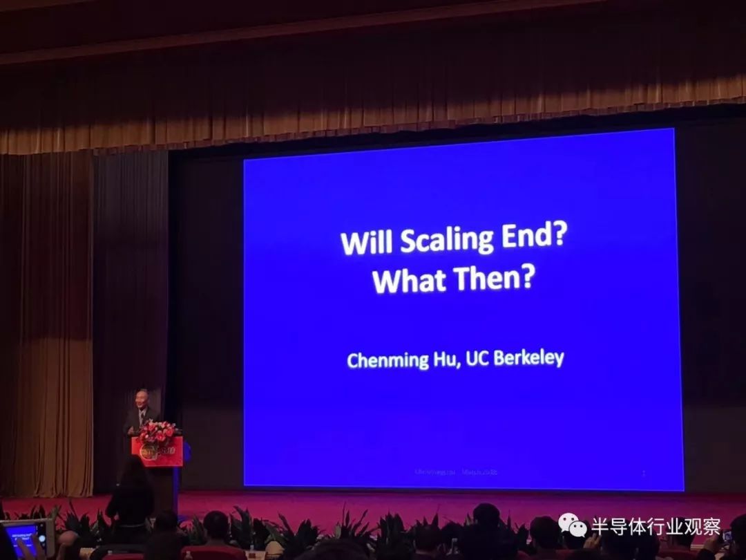
In the process of upgrading the manufacturing process of integrated circuits, the emergence of High-K and FinFET played an important role in the continuation of Moore's Law, and repeatedly broke the predictions of experts in the past. In recent years, with the further evolution of the process, the industry has begun to have doubts about whether the transistor can continue to indent.
At the CSTIC2018 opening today, Professor FinFET's inventor, Professor Hu Zhengming, published the title "Will Scaling End?" What Then? The speech of the development of integrated circuit manufacturing.

Professor Hu said that in 1999, the general view of the industry was that transistor miniaturization would end at 35 nm.

However, in the same year, UC Berkeley introduced a 45-nm FinFET transistor. Thanks to the new transistor construction mode, the device's performance test parameters have achieved good results.

At the time, Professor Hu Zhengming discovered that even though the 1 nm oxide layer could not eliminate the leakage at several nanometers below the interface, they proposed two Ultra-thin-body MOSFETs to DARPA.


One of them is the FinFET that changes the history of the entire semiconductor:

Another structure is UTB-SOI (FDSOI):


When it comes to limiting Lg miniaturization, silicon's film/fin/wire can be reduced to 6nm, according to the ITRS.
However, the natural thickness of crystals such as MoS2, WSe, and HfTE is 0.6 nm. 2D transistors based on these materials have shorter Lg and better electrical properties, but the fabrication process is difficult and wants to grow evenly on a 12-inch wafer. In fact, there are big challenges.


He further pointed out that Full wafer available Seeded CVD MOS2 over SiO2

After Professor Hu introduced the stacked 2D semiconductor circuit

Also mentioned is the FinFET in which the CVD MoS2 channel is placed on the fin Si back gate.

Professor Hu stressed the importance of reducing IC power consumption

To achieve the goal of reducing power consumption, you need to consider the following three directions:

First he shared his opinion on lowering Vdd.

Then Professor Hu also talked about negative capacitance transistors (NCFETs).

He compared the 30nm FinFET with the NCFET

And further emphasize the characteristics of NCFET

Professor Hu also introduced Ferroelectric Negative Capacitance.

Also made a performance comparison at different voltages

He also summarized the following points

Professor Hu said that transistor miniaturization will become slower and slower.
On the one hand, because the size of the atoms is fixed, physical limits are reached; on the other hand, lithography and other manufacturing techniques are becoming more and more expensive. But with device innovation, cost-power-speed can continue to improve.

The entire semiconductor industry will certainly grow in the long run. Not everyone will benefit, there are losers and winners, but because of the large amount of semiconductors, the winner will be very successful. In the past few years, semiconductor output has surpassed all sums before 1995, and semiconductor growth will not be slower than global economic growth because people need smarter equipment.

Finally, Professor Hu made a summary of his speech:


Stylus Pen Tip,Stylus Pencil Tip,Carbon Fiber Pen Tip,Carbon Fiber Stylus Pen Tip
Shenzhen Ruidian Technology CO., Ltd , https://www.szwisonen.com